Up/down counter (16 bit mode), Chapter 41 up/down counter 3.configuration, Udcr1 udcr0 udrc1 udrc0 – FUJITSU MB91460 SERIES FR60 User Manual
Page 854: Udc0 interrupt (#128), 16 bit mode, Peripheral clock clkp
838
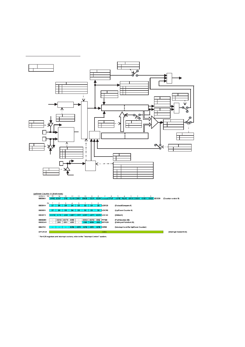
Chapter 41 Up/Down Counter
3.Configuration
Figure 3-3 Configuration Diagram
Figure 3-4 Register List
Note: For ICR registers and interrupt vectors, refer to “
Chapter 24 Interrupt Control (Page No.311)
UDCR1
UDCR0
UDRC1
UDRC0
UDC0 interrupt
(#128)
CMPF
UDCS0: bit4
0
1
Compare match
No compare match
CITE
UDCS0: bit6
0
1
Disable interrupts
Enable interrupts
CMS1-0
UDCC0: bit11-10
Timer mode (Countdown only)
0
0
1
1
0
1
1
0
Up/down count mode
Phase difference count mode (Multiply by 2)
Phase difference count mode (Multiply by 4)
UDCC0: bit1-0, bit 2
CGE1-0
0
0
1
1
0
1
1
0
Disable edge detection
Enable falling edge detection
Enable rising edge detection
Disable setting
Disable level detection
Enable LOW level detection
Enable HIGH level detection
Disable setting
1: Gate function
CGSC
UDCC0: bit2
0
1
Counter clear
No impact
UDIE
UDCS0: bit5
0
1
Disable interrupts
Enable interrupts
UDFF
UDCS0: bit2
0
1
No underflow
Underflowed
CSTR
UDCS0: bit7
0
1
Stop counting
Start counting
Activation
CTUT
UDCC0: bit6
0
1
No impact
Data transfer
* Only 16 bit transfer is enabled
while counting stops.
CDCF
UDCC0: bit14
0
1
No change direction
Direction changed
CFIE
UDCC0: bit 13
0
1
Disable interrupts
Enable interrupts
CLKS
UDCC0: bit 12
0
1
CLKP divided by 2
CLKP divided by 8
16 bit mode
M16E
UDCC0 : bit15
1
16 bit mode
OR
OR
Up/Down Counter (Read only)
Reload/compare register (Write only)
Reload
1
1
0
0
1
0
UDF1-0
UDCS0: bit 1 -0
No input
0
0
1
1
0
1
1
0
Countdown
Countup
Both countdown and countup
Write: Disabled, Read only
1
0
CES1-0
UDCC0: bit 9 -8
0
0
1
1
0
1
1
0
Disable edge detection
Enable falling edge detection
Enable rising edge detection
Enable both edge detection
From port data
register
From port data
register
From port data
register
BIN0/SOT2/P20.1
ZIN0/SCK2/P20.2
P20 EPFR20.1
0
1
Others
Enable UDC
AIN0/SIN2/P20.0
P20 EPFR20.0
0
1
Others
Enable UDC
P20 EPFR20.2
0
1
Others
Enable UDC
Com-
pare
OR
Up/Down Counter (16 Bit Mode)
UCRE
UDCC0:bit5
0
1
Disable counter clear
Enable counter clear
1
0
RLDE
UDCC0: bit4
0
1
Disable reload
Enable reload
Peripheral clock
CLKP
Gate
Read from port
Read from
port
WRITE 0: Flag clear
OVFF
UDCS0: bit3
0
1
No overflow
Overflowed
WRITE 0: Flag clear
WRITE 0: Flag clear
WRITE 0: Flag clear
0
0
-
0: Counter clear function
0
0
0
0
OR
Counter clear
UDF1-0
-
Prescaler
Selector
0
Edge
detection
OR
0
0
Edge
detection
Read
from
port