FUJITSU MB91460 SERIES FR60 User Manual
Page 466
450
Chapter 30 I/O Ports
1.I/O Ports Functions
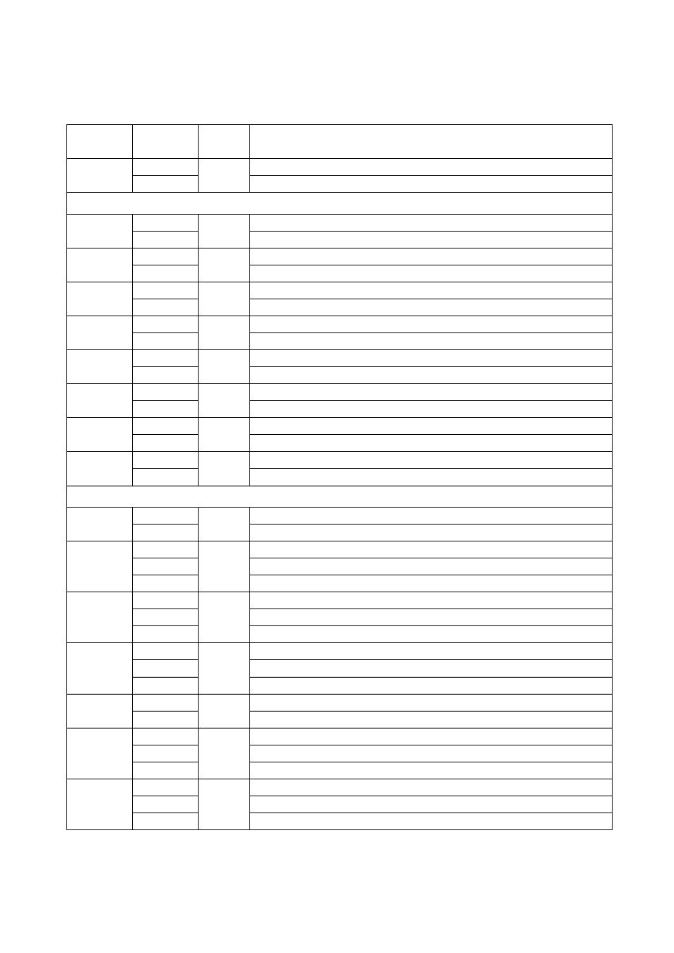
P30_0
P30_0
TP06_0
General purpose I/O.
COM0
Common driver output pin 0 LCD controller.
Port 31
P31_7
P31_7
TP06_0
General purpose I/O.
SEG39
Segment driver output pin 39 LCD controller.
P31_6
P31_6
TP06_0
General purpose I/O.
SEG38
Segment driver output pin 38 LCD controller.
P31_5
P31_5
TP06_0
General purpose I/O.
SEG37
Segment driver output pin 37 LCD controller.
P31_4
P31_4
TP06_0
General purpose I/O.
SEG36
Segment driver output pin 36 LCD controller.
P31_3
P31_3
TP06_0
General purpose I/O.
SEG35
Segment driver output pin 35 LCD controller.
P31_2
P31_2
TP06_0
General purpose I/O.
SEG34
Segment driver output pin 34 LCD controller.
P31_1
P31_1
TP06_0
General purpose I/O.
SEG33
Segment driver output pin 33 LCD controller.
P31_0
P31_0
TP06_0
General purpose I/O.
SEG32
Segment driver output pin 32 LCD controller.
Port 32
P32_7
P32_7
TP06_0
General purpose I/O.
SEG31
Segment driver output pin 31 LCD controller.
P32_6
P32_6
TP06_0
General purpose I/O.
SEG30
Segment driver output pin 30 LCD controller.
SCK15
Clock I/O pin for LIN-USART 15.
P32_5
P32_5
TP06_0
General purpose I/O.
SEG29
Segment driver output pin 29 LCD controller.
SOT15
Serial data output pin for LIN-USART 15.
P32_4
P32_4
TP06_0
General purpose I/O.
SEG28
Segment driver output pin 28 LCD controller.
SIN15
Serial data input pin for LIN-USART 15.
P32_3
P32_3
TP06_0
General purpose I/O.
SEG27
Segment driver output pin 27 LCD controller.
P32_2
P32_2
TP06_0
General purpose I/O.
SEG26
Segment driver output pin 26 LCD controller.
SCK14
Clock I/O pin for LIN-USART 14.
P32_1
P32_1
TP06_0
General purpose I/O.
SEG25
Segment driver output pin 25 LCD controller.
SOT14
Serial data output pin for LIN-USART 14.
Pin Name
I/O Signal
Circuit
Type
Function