2 clkr: clock source control register – FUJITSU MB91460 SERIES FR60 User Manual
Page 268
252
Chapter 18 Timebase Counter
4.Registers
4.2 CLKR: Clock Source Control Register
Selects the clock source for the base clock used to run the MCU and controls the PLL.
Note: See also the “
Chapter 13 Clock Control (Page No.189)
”.
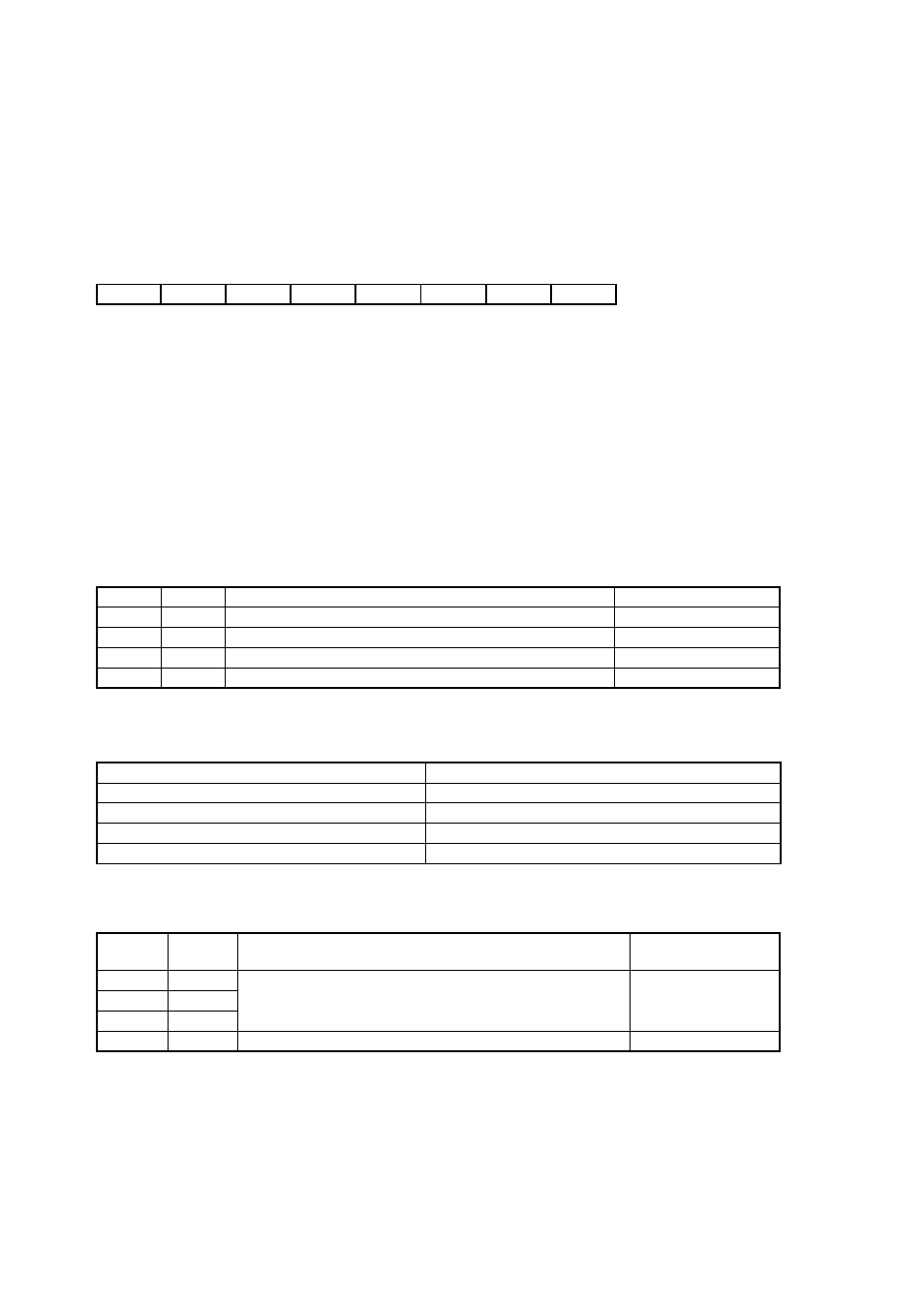
• CLKR: Address 0484h (Access: Byte)
Meaning of Bit Attribute Symbols (Page No.10)
” for details of the attributes.)
• Bit7-4: Reserved bit Always write “0” to this bit. The read value is the value written.
• Bit3: Subclock selection enable (SCKEN)
• Setting this bit to “1” enables the subclock to be selected.
• Bit2: Main PLL operation enable (PLL1EN)
• Setting this bit to “1” starts main PLL operation. Main PLL can be selected as the operating clock after the
main PLL has locked.
• Bit1-0: Clock source selection
When changing the clock mode, the value of CLKS0 cannot be modified if CLKS1 is “1”
The table below lists the cases when the CLKS1 - CLKS0 bits may or may not be modified.
Example: To select the subclock after an INIT reset, first write “01
B
” and then write “11
B
” (subclock)
The clock source for the timebase counter during the oscillation stabilization wait time is set by the clock source
selection bits.
7
6
5
4
3
2
1
0
bit
-
-
-
-
SCKEN
PLL1EN
CLKS1
CLKS0
X
X
X
X
0
0
0
0
Initial value
(INIT pin input)
X
X
X
X
X
X
X
X
Initial value
(
Software reset
)
R/W0
R/W0
R/W0
R/W0
R/W
R/W
R/W
R/W
Attribute
CLKS1
CLKS0
Clock source setting
Mode
0
0
The main clock input from X0/X1 divided by 2 (initial value)
Main clock mode
0
1
The main clock input from X0/X1 divided by 2
Main clock mode
1
0
Main PLL
Main clock mode
1
1
Subclock
Subclock mode
Table 4-1 Cases When the CLKS1 and CLKS0 Bits May or May Not be Modified
Modify permitted
Modify not permitted
“00” -> “01” or “10”
“00” -> “11”
“01” -> “11” or “00”
“01” -> “10”
“10” -> “00”
“10” -> “01” or “11”
“11” -> “01”
“11” -> “00” or “10”
CLKS1
CLKS0
Clock source for timebase
counter during oscillation stabilization wait time
Mode
0
0
The main clock input from X0/X1 divided by 2 (initial value)
Main clock mode
0
1
1
0
1
1
Subclock
Subclock mode