Configuration, D/a converter (0-1), Avss avcc – FUJITSU MB91460 SERIES FR60 User Manual
Page 926
910
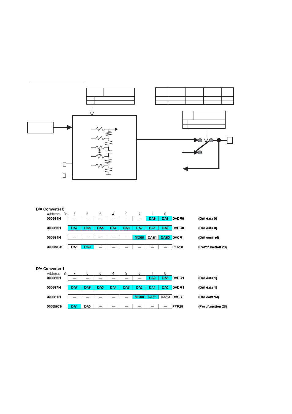
Chapter 45 D/A Converter
3.Configuration
3. Configuration
Figure 3-1 Configuration Diagram
For a detailed description of the D/A pin circuit, see the chapter entitled “Basic Information”.
Figure 3-2 Register List
2
2
2
2R
2
2
D/A converter (0-1)
DA0/P28.6
DA1/P28.7
DADR0/
DADR1
DA0
DA1
PFR28: bit 6
PFR28: bit 7
0
1
General-purpose port output
D/A output only
1
0
DAE
0
1
D/A output disable (0 V output)
D/A output enable
DACR: bit 0
DACR: bit 1
AVss
AVcc
From Port
Data register
Port read
Register number (:bit)
Data
Control
Port
function
DADR0
DACR.DAE0
PFR28.6
DADR1
PFR28.7
D/A
0
1
Pin
DA0
DA1
R
R
R
R
R
R
R
2
R
DACR.DAE1
See also other documents in the category FUJITSU Hardware:
- XG Series P3NK-4452-01ENZD (614 pages)
- FPCAC14C (1 page)
- MCJ3230SS (161 pages)
- MBA3073NC (138 pages)
- T5140 (76 pages)
- T5140 (102 pages)
- MAM3367MC/MP (152 pages)
- MPC3045AH (185 pages)
- MB2142-02 (23 pages)
- MB15F86UL (6 pages)
- MHS2030AT (40 pages)
- MHW2100BS (296 pages)
- MHK2060AT (227 pages)
- Disk Drives MHK2060AT (227 pages)
- MCM3064SS (170 pages)
- Mainboard D1561 (45 pages)
- MHC2040AT (219 pages)
- D1961 (45 pages)
- DISK DRIVES MHM2100AT (231 pages)
- MHR2010AT (250 pages)
- MHZ2120BJ (320 pages)
- MCE3064AP (175 pages)
- LQFP-64P (16 pages)
- Solaris PCI GigabitEthernet 3.0 (115 pages)
- MAY2036RC (94 pages)
- MAB3091 (142 pages)
- MPE3XXXAT (191 pages)
- MHV2040AH (40 pages)
- MHW2040AC (278 pages)
- ETERNUSmgr P2X0-0202-01EN (64 pages)
- VSS Hardware Provider 2.1 (134 pages)
- MAG3182FC (61 pages)
- MAU3147NC/NP (130 pages)
- MAX3147RC (94 pages)
- MHV2160BT (296 pages)
- MHV2040AT (280 pages)
- MAW3300NC/NP (130 pages)
- DeskPower E623 (50 pages)
- MAG3182LC (133 pages)
- OPTICAL DISK DRIVES MDG3064UB (42 pages)
- MHF2021AT (225 pages)
- MHR2040AT (40 pages)
- Single Drive FTM7926FB (1 page)
- PG-FCS103 (98 pages)
- MAS3735FC (114 pages)