Figure 10-1, Timing – FUJITSU MB91460 SERIES FR60 User Manual
Page 609
593
Chapter 31 External Bus
10.DMA Access Operation
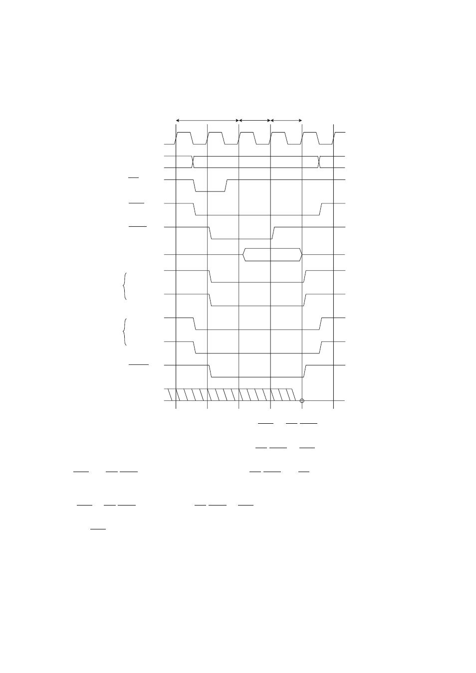
Figure 10-1 Timing Chart for DMA Fly-By Transfer (I/O -> Memory)
•
Setting 1 for the W01 bit of the AWR register enables the CSn -> RD/WRn setup delay to be set. Set this bit
to extend the period between assertion of chip select and the read/write strobe.
•
Setting 1 for the W00 bit of the AWR register enables the RD/WRn -> CSn hold delay to be set. Set this bit to
extend the period between negation of the read/write strobe and negation of chip select.
•
nThe CSn -> RD/WRn setup delay (W01 bit) and RD/WRn -> CS hold delay (W00 bit) can be set
independently.
•
When successive accesses are made within the same chip select area without negating the chip select,
neither CSn -> RD/WRn setup delay nor RD/WRn -> CSn hold delay is inserted.
•
If a setup cycle for determining the address or a hold cycle for determining the address is needed, set 1 for the
address -> CSn delay setting (W02 bit of the AWR register).
For I/O on the data output side, a read strobe of three bus cycles extended by the I/O wait cycle and I/O hold wait
cycle is generated. For memory on the receiving side, a write strobe of two bus cycles extended by the I/O wait
cycle is generated. The I/O hold wait cycle does not affect the write strobe. However, the address and CS signal
are retained until the fly-by bus access cycles end.
DACKn
DEOPn
DACKn
DEOPn
IORD
DREQn
FR30
compatible
mode
Basic
mode
memory address
MCLK
AS
CSn
A[31:0]
D[31:0]
WRn
Sense timing in
demand mode
I/O wait I/O hold
Basic cycle cycle wait
n = 0, 1, 2