Explanation of the different blocks, Figure 2-1 usart block diagram – FUJITSU MB91460 SERIES FR60 User Manual
Page 633
617
Chapter 32 USART (LIN / FIFO)
2.USART Configuration
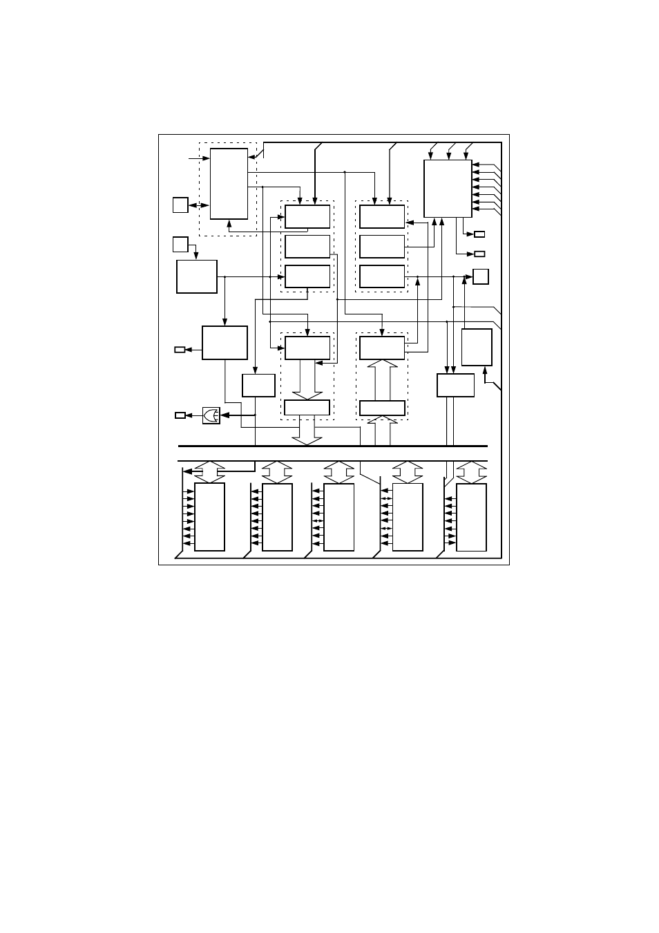
Figure 2-1 USART Block Diagram
■
Explanation of the different blocks
• Reload Counter
The reload counter functions as the dedicated baud rate generator. It can select external input clock or internal
clock for the transmitting and receiving clocks. The reload counter has a 15 bit register for the reload value.
The actual count of the transmission reload counter can be read via the BGR0/1 registers.
• Reception Control Circuit
The reception control circuit consists of a received bit counter, start bit detection circuit, and received parity
counter. The received bit counter counts reception data bits. When reception of one data item for the specified
data length is complete, the received bit counter sets the Reception data register full flag. When the FIFO is
enabeld, the flag is set if the triggerlevel is reached. The start bit detection circuit detects start bits from the
serial input signal and sends a signal to the reload counter to synchronize it to the falling edge of these start
bits. The reception parity counter calculates the parity of the reception data.
• Reception Shift Register
The reception shift register fetches reception data input from the SIN04 pin, shifting the data bit by bit. When
reception is complete, the reception shift register transfers receive data to the RDR04 register.
RDR (FIFO
TDR (FIFO)
Reception
shift register
Transmission
shift register
Received
Parity counter
Received
Bit counter
Start bit
Detection
circuit
Transmission
Start circuit
Transmission
Bit counter
Transmission
Parity counter
Pin
Internal data bus
register
register
register
register
PEN
P
SBL
CL
A/D
CRE
RXE
TXE
MD1
MD0
(OTO)
(EXT)
(REST)
SCKE
SOE
PE
ORE
FRE
RDRF
TDRE
BDS
RIE
TIE
LBIE
LBD
SOPE
SIOP
CCO
SCES
LIN break
Detection
circuit
Bus idle
Detection
circuit
Pin
Pin
Error
Detection
transmission clock
reception clock
Interrupt
Generation
circuit
LBIE
LBD
BIE
RBI
RIE
TIE
reception
IRQ
transm.
IRQ
RECEPTION
CONTROL
CIRCUIT
TRANSMISSION
CONTROL
CIRCUIT
reception
complete
transmission
start
LBD
SIN
PE
ORE FRE
CLK
SIN
SOT
register
LBR
MS
SSM
BIE
SCDE
TDRE
RDRF
RBI
TBI
UPCL
LBL1
LBL0
(OTO,
EXT,
REST)
and Synch
Field
LIN
break
genera-
tion
circuit
LBR
LBL1
LBL0
PE
ORE
FRE
TBI
Over-
sampling
Unit
RBI
TBI
Signal
to EI
2
OS
Signal
to ICU
Counter
Reload
Restart Reception
Reload Counter
SIN0
SCK0
SOT0
SSR
SSR
SCR0
ESCR
ECCR