Configuration, Chapter 47 lcd controller 3.configuration, Lcd controller – FUJITSU MB91460 SERIES FR60 User Manual
Page 938
922
Chapter 47 LCD Controller
3.Configuration
3. Configuration
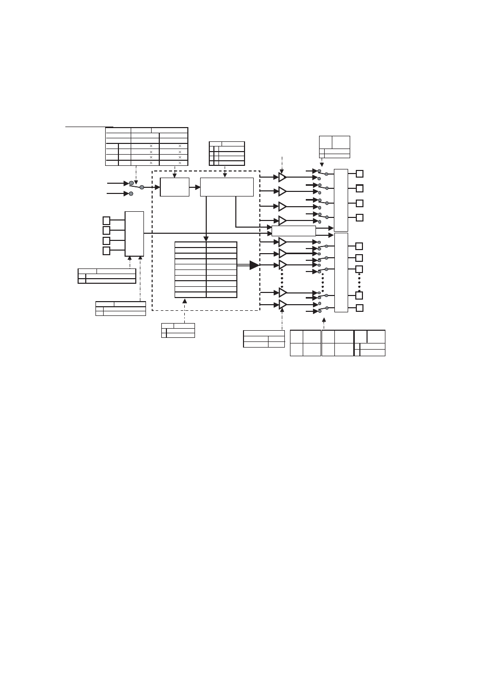
Figure 3-1 Configuration Diagram
Note: For details on ports, refer to “
Chapter 30 I/O Ports (Page No.431)
” and “
Chapter 3 MB91460 Series Basic
Timing
Control Circuit
LCDCMR
Initial value
Setting
---- 0000
00001111
LCR1
Initial value
Setting
00 00000000
11 11111111
MS1,0 LCR0: bit3,2
1 1/4 duty cycle
1
0 1/3 duty cycle
1
1 1/2 duty cycle
0
0
Deactivate
0
BK
LCR0: bit4
0
Display
1
Blank
LCEN
LCR0: bit6
1
Enable display in watch mode.
0
Disable display in watch mode.
VSEL
LCR0: bit5
1
Connect internal divided resistors.
0
Disconnect internal divided resistors.
Internal
Divided
Resistors
0
1
Peripheral
clock
Sub
clock
Prescaler
VRAM 0
VRAM 1
VRAM 2
VRAM 3
VRAM 4
VRAM 5
VRAM 6
VRAM 7
VRAM 8
VRAM 9
VRAM 10
VRAM 11
VRAM 12
VRAM 13
VRAM 14
VRAM 15
SEG32
:
SEG39
PFR31.0
:
PFR31.7
0
1
SEG output
General-purp. port
SEG24
:
SEG31
PFR32.0
:
PFR32.7
SEG16
:
SEG23
PFR33.0
:
PFR33.7
SEG8
:
SEG15
PFR34.0
:
PFR34.7
SEG0
:
SEG7
PFR35.0
:
PFR35.7
COM0
:
COM3
PFR30.0
:
PFR30.3
0
1
General-purp. ports
COM output
From port data
register
COM3
COM1
COM2
COM0
SEG0
1
SEG1
SEG30
SEG39
SEG2
From
general-purpose
port register
CSS
LCR0: bit7
1
Subclock
0
Main clock
FP1,0
LCR0: bit1,0
F
CLKP
/(2
16
N)
F
CLKP
/(2
15
N)
F
CLKP
/(2
14
N)
F
CLKP
/(2
13
N)
1
1
0
1
1
0
0
0
F
CL-SUB
/(2
6
N)
F
CL-SUB
/(2
5
N)
F
CL-SUB
/(2
4
N)
F
CL-SUB
/(2
3
N)
V0
V1
V2
V3
LCD Controller
LCDCMR
:
0
:
:
:
:
:
:
:
:
:
0
AC Circuit
Control Section
1
0
FP1,0
0
0
Common Driver
Segment Driver
VRAM16
VRAM17
VRAM18
VRAM19