Figure 5-11, Timing – FUJITSU MB91460 SERIES FR60 User Manual
Page 589
573
Chapter 31 External Bus
5.Operation of the Ordinary bus interface
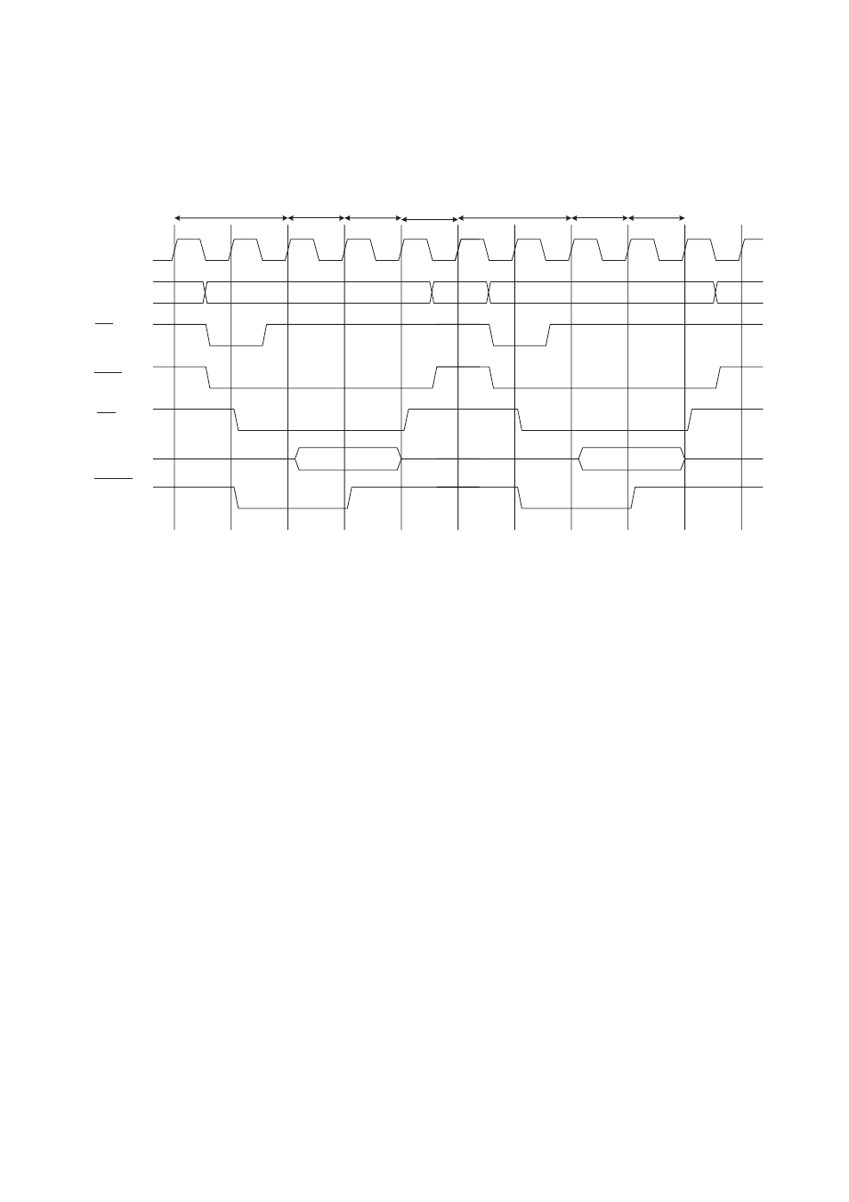
Figure 5-11 Timing Chart for DMA Fly-By Transfer (Memory -> I/O)
•
Setting 1 for the HLD bit of the IOWR0-3 registers enables the I/O read cycle to be extended by one cycle.
•
Setting the WR1,0 bits of the IOWR0-3 registers enables 0-3 write recovery cycles to be inserted.
•
If the write recovery cycle is set to 1 or more, a write recovery cycle is always inserted after write access.
•
Setting bits IW3-0 of the IOWR0-3 registers enables 0-15 wait cycles to be inserted.
•
If wait is also set on the memory side (AWR15-12 is not 0), the larger value is used as the wait cycle after
comparison with the I/O wait (IW3-0 bits).
RD
IOWR
MCLK
AS
CSn
D[31:0]
A[31:0]
Basic cycle
Basic cycle
I/O wait
cycle *1
I/O hold
wait *2
I/O wait
cycle *1
I/O hold
wait *2
I/O idle
cycle
- XG Series P3NK-4452-01ENZD (614 pages)
- FPCAC14C (1 page)
- MCJ3230SS (161 pages)
- MBA3073NC (138 pages)
- T5140 (102 pages)
- T5140 (76 pages)
- MAM3367MC/MP (152 pages)
- MPC3045AH (185 pages)
- MB2142-02 (23 pages)
- MB15F86UL (6 pages)
- MHS2030AT (40 pages)
- MHW2100BS (296 pages)
- MHK2060AT (227 pages)
- Disk Drives MHK2060AT (227 pages)
- MCM3064SS (170 pages)
- Mainboard D1561 (45 pages)
- MHC2040AT (219 pages)
- D1961 (45 pages)
- DISK DRIVES MHM2100AT (231 pages)
- MHR2010AT (250 pages)
- MHZ2120BJ (320 pages)
- MCE3064AP (175 pages)
- LQFP-64P (16 pages)
- Solaris PCI GigabitEthernet 3.0 (115 pages)
- MAY2036RC (94 pages)
- MAB3091 (142 pages)
- MPE3XXXAT (191 pages)
- MHV2040AH (40 pages)
- MHW2040AC (278 pages)
- ETERNUSmgr P2X0-0202-01EN (64 pages)
- VSS Hardware Provider 2.1 (134 pages)
- MAG3182FC (61 pages)
- MAU3147NC/NP (130 pages)
- MAX3147RC (94 pages)
- MHV2160BT (296 pages)
- MHV2040AT (280 pages)
- MAW3300NC/NP (130 pages)
- DeskPower E623 (50 pages)
- MAG3182LC (133 pages)
- OPTICAL DISK DRIVES MDG3064UB (42 pages)
- MHF2021AT (225 pages)
- MHR2040AT (40 pages)
- Single Drive FTM7926FB (1 page)
- PG-FCS103 (98 pages)
- MAS3735FC (114 pages)