Chapter 25 external interrupt 3.configuration – FUJITSU MB91460 SERIES FR60 User Manual
Page 339
323
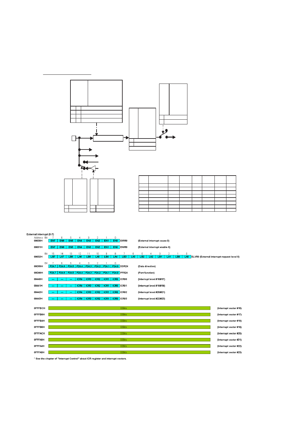
Chapter 25 External Interrupt
3.Configuration
Figure 3-2 Configuration Diagram
Figure 3-3 Register List
External interrupts 8 - 15
LB8, LA8
LB9, LA9
LB10, LA10
LB11, LA11
LB12, LA12
LB13, LA13
LB14, LA14
LB15, LA15
ELVR1 : bit 1-0,
ELVR1 : bit 3-2,
ELVR1 : bit 5-4,
ELVR1 : bit 7-6,
ELVR1 : bit 9-8,
ELVR1 : bit 11-10,
ELVR1 : bit 13-12,
ELVR1 : bit 15-14
Detect level setting
0
0
1
1
0
1
1
0
INT8/RX0/P23.0
INT9/RX1/P23.2
INT10/RX2/P23.4
INT11/RX3/P23.6
INT12/RX4/P22.0
INT13/RX5/P22.2
INT14/SDA0/P22.4
INT15/SDA1/P22.6
Edge detection circuit
Pins
Detect at the rising edge
Detect at the falling edge
External interrupt request flag
ER0,
ER1,
ER2,
ER3,
ER4,
ER5,
ER6,
ER7
EIRR1: bit n0
EIRR1: bit n1
EIRR1: bit n2
EIRR1: bit n3
EIRR1: bit n4
EIRR1: bit n5
EIRR1: bit n6
EIRR1: bit n7
0
1
No interrupt requests
Interrupt request present
WRITE 0: Flag clear
Register number
External
interrupt
8
9
10
11
12
13
14
15
External interrupt
request level
setting bit
LB8, LA8
LB9, LA9
LB10, LA10
LB11, LA11
LB12, LA12
LB13, LA13
LB14, LA14
LB15, LA15
External
interrupt
request bit
ER8
ER9
ER10
ER11
ER12
ER13
ER14
ER15
Enable external
interrupt
requests
EN8
EN9
EN10
EN11
EN12
EN13
EN14
EN15
Interrupt
number
#24
#25
#26
#27
#28
#29
#30
#31
The data
direction bit
P23.0
P23.2
P23.4
P23.6
P22.0
P22.2
P22.4
P22.6
Pins
Port
function
INT8
INT9
INT10
INT11
RX3
INT12
INT13
INT14
INT15
External interrupt request enable flag
EN0,
EN1,
EN2,
EN3,
EN4,
EN5,
EN6,
EN7
ENIR1 : bit 0
ENIR1 : bit 1
ENIR1 : bit 2
ENIR1 : bit 3
ENIR1 : bit 4
ENIR1 : bit 5
ENIR1 : bit 6
ENIR1 : bit 7
0
1
Disable interrupts
Enable interrupts
Interrupt request
(#24, #25, #26, #27
#28, #29, #30, #31)
Detect at
“L”
level
Detect at
“H”
level
RX0
RX1
RX2
RX4
RX5
SDA0
SDA1
P23.0
P23.2
P23.4
P23.6
P22.0
P22.2
P22.4
P22.6
DDR23: bit0
DDR23: bit2
DDR23: bit4
DDR23: bit6
DDR22: bit0
DDR22: bit2
DDR22: bit4
DDR22: bit6
0
1
Input only
Enable output
0
RX0
RX1
PFR23: bit0
PFR23: bit2
1
General-purpose port
Peripheral
RX2
RX3
PFR23: bit4
PFR23: bit6
PFR22: bit0
PFR22: bit2
PFR22: bit4
PFR22: bit6
RX4
RX5
SDA0
SDA1
1
0
(Inputs of other peripheral
function macros)
Read of the port
(Outputs of other peripheral function macros)
From the port data register