Sdram interface, 1 big endian bus access, Word access (when ld/st instruction executed) – FUJITSU MB91460 SERIES FR60 User Manual
Page 560
544
Chapter 31 External Bus
4.Endian and Bus Access
●
SDRAM Interface
Figure 4-3 Data bus width of the SDRAM (FCRAM) interface and its control signals
4.1 Big Endian Bus Access
With the exception of the CS0 area of the MB91460 series, either the big endian method or the
little endian method can be selected for each chip select area. If 0 is set for the LEND bit of the
ACR register, the area is treated as big endian. The MB91460 series is normally big endian and
performs external bus access.
■
Data Format
The relationship between the internal register and the external data bus is as follows:
●
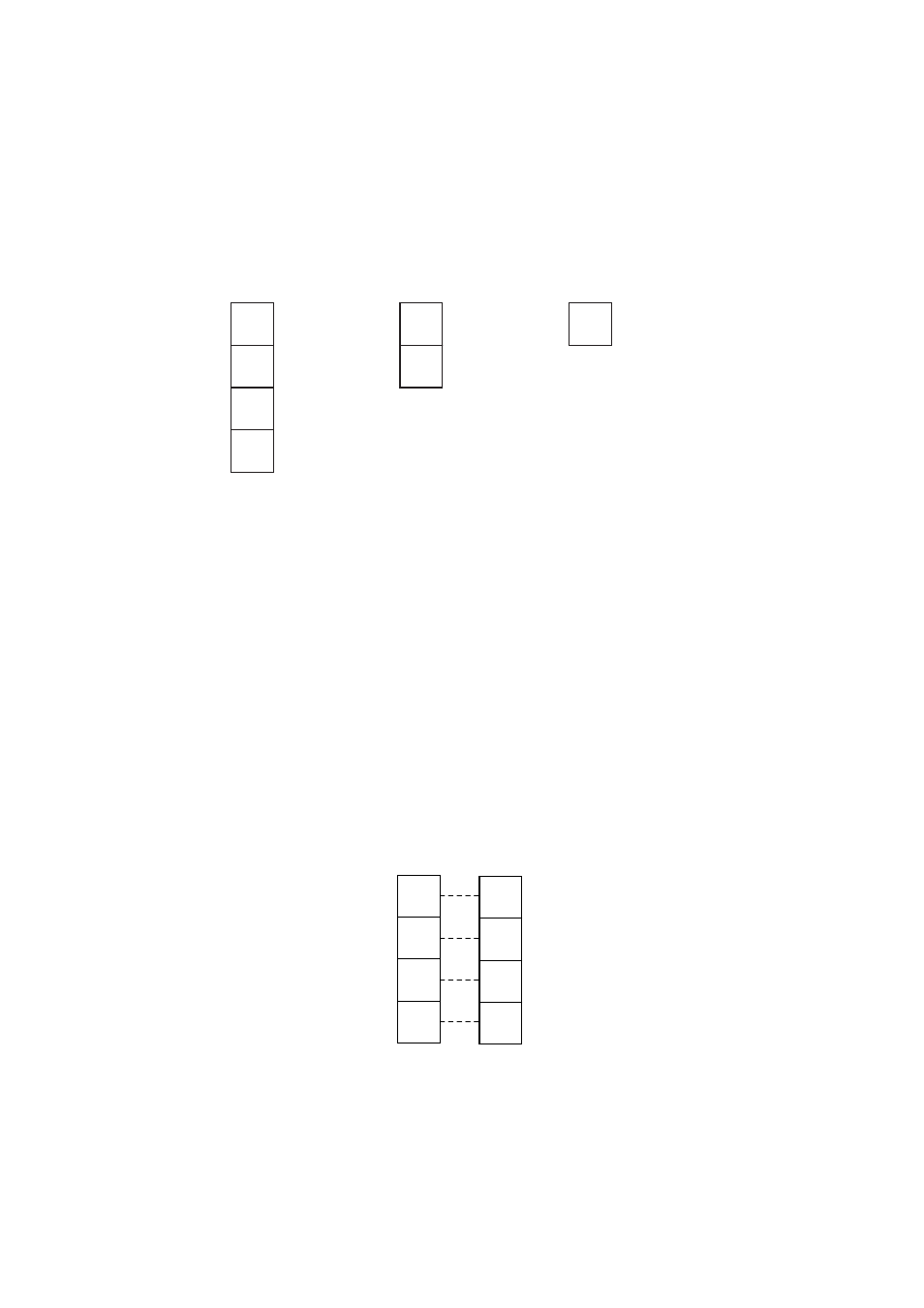
Word access (when LD/ST instruction executed)
Figure 4-4 Relationship between Internal Register and External Data Bus for Word Access
D31
D0
a)32-bit bus width
Data bus
Control signal
DQMUU
DQMUL
DQMLU
DQMLL
Data bus
Control signal
Data bus
Control si
DQMUU
DQMUL
DQMUU
-
-
-
-
-
b)16-bit bus width
c)8-bit bus width
-
-
-
-
-
(D15 to 0 are not used.)
(D23 to 0 are not used.)
D31
D15
D23
D7
D0
AA
BB
CC
DD
Internal register
D31
D15
D23
D7
D0
AA
BB
CC
DD
External register