FUJITSU MB91460 SERIES FR60 User Manual
Page 461
445
Chapter 30 I/O Ports
1.I/O Ports Functions
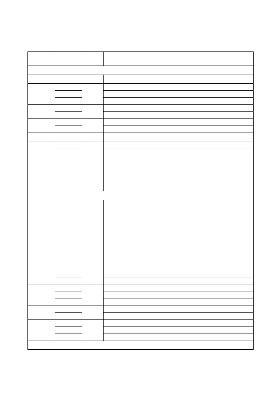
Port 21
P21_7
P21_7
TP00_0
General purpose I/O.
P21_6
P21_6
TP00_0
General purpose I/O.
SCK1
Clock I/O pin for LIN-USART 1.
CK1
Input for the 16-bit I/O Timer FRT 1.
P21_5
P21_5
TP00_0
General purpose I/O.
SOT1
Serial data output pin for LIN-USART 1.
P21_4
P21_4
TP00_0
General purpose I/O.
SIN1
Serial data input pin for LIN-USART 1.
P21_3
P21_3
TP00_0
General purpose I/O.
P21_2
P21_2
TP00_0
General purpose I/O.
SCK0
Clock I/O pin for LIN-USART 0.
CK0
Input for the 16-bit I/O Timer FRT 0.
P21_1
P21_1
TP00_0
General purpose I/O.
SOT0
Serial data output pin for LIN-USART 0.
P21_0
P21_0
TP00_0
General purpose I/O.
SIN0
Serial data input pin for LIN-USART 0.
Port 22
P22_7
P22_7
TP02_0
General purpose I/O.
SCL1
Serial clock I/O pin for I2C 1.
P22_6
P22_6
TP02_0
General purpose I/O.
SDA1
Serial data I/O pin for I2C 1.
INT15
External interrupt request input pin for INT 15.
P22_5
P22_5
TP02_0
General purpose I/O.
SCL0
Serial clock I/O pin for I2C 0.
P22_4
P22_4
TP02_0
General purpose I/O.
SDA0
Serial data I/O pin for I2C 0.
INT14
External interrupt request input pin for INT 14.
P22_3
P22_3
TP00_0
General purpose I/O.
TX5
Transmission output pin for CAN 5.
P22_2
P22_2
TP00_0
General purpose I/O.
RX5
Reception input pin for CAN 5.
INT13
External interrupt request input pin for INT 13.
P22_1
P22_1
TP00_0
General purpose I/O.
TX4
Transmission output pin for CAN 4.
P22_0
P22_0
TP00_0
General purpose I/O.
RX4
Reception input pin for CAN 4.
INT12
External interrupt request input pin for INT 12.
Port 23
Pin Name
I/O Signal
Circuit
Type
Function