3 lcr1: lcdc control register 1, 4 lcdcmr: common pin switching register – FUJITSU MB91460 SERIES FR60 User Manual
Page 944
928
Chapter 47 LCD Controller
4.Registers
4.3 LCR1: LCDC Control Register 1
• LCR1H: Address 0EA
H
(Access: Byte, Half-word, Word)
(For attributes, refer to “
Meaning of Bit Attribute Symbols (Page No.10)
• bit15-10: Undefined (Read: Indeterminate, Write: “0” is always written.)
• bit9-8: Segment driver enable.
Always set to “11
B
” when LCD is used.
• LCR1L: Address 0EB
H
(Access: Byte, Half-word, Word)
(For attributes, refer to “
Meaning of Bit Attribute Symbols (Page No.10)
• bit7-0: Segment driver enable.
When LCD is used, always set this register to “11111111
B
”.
4.4 LCDCMR: Common Pin Switching Register
• LCDCMR: Address 0E8
H
(Access: Byte, Half-word, Word)
(For attributes, refer to “
Meaning of Bit Attribute Symbols (Page No.10)
• bit7: Analogue macro control.
Always set to “0
B
” when LCD is used.
• bit6-4: Undefined (Read: Indeterminate, Write: “0” is always written.)
• bit3-0: Common driver enable.
Always set to “1111
B
” when LCD is used.
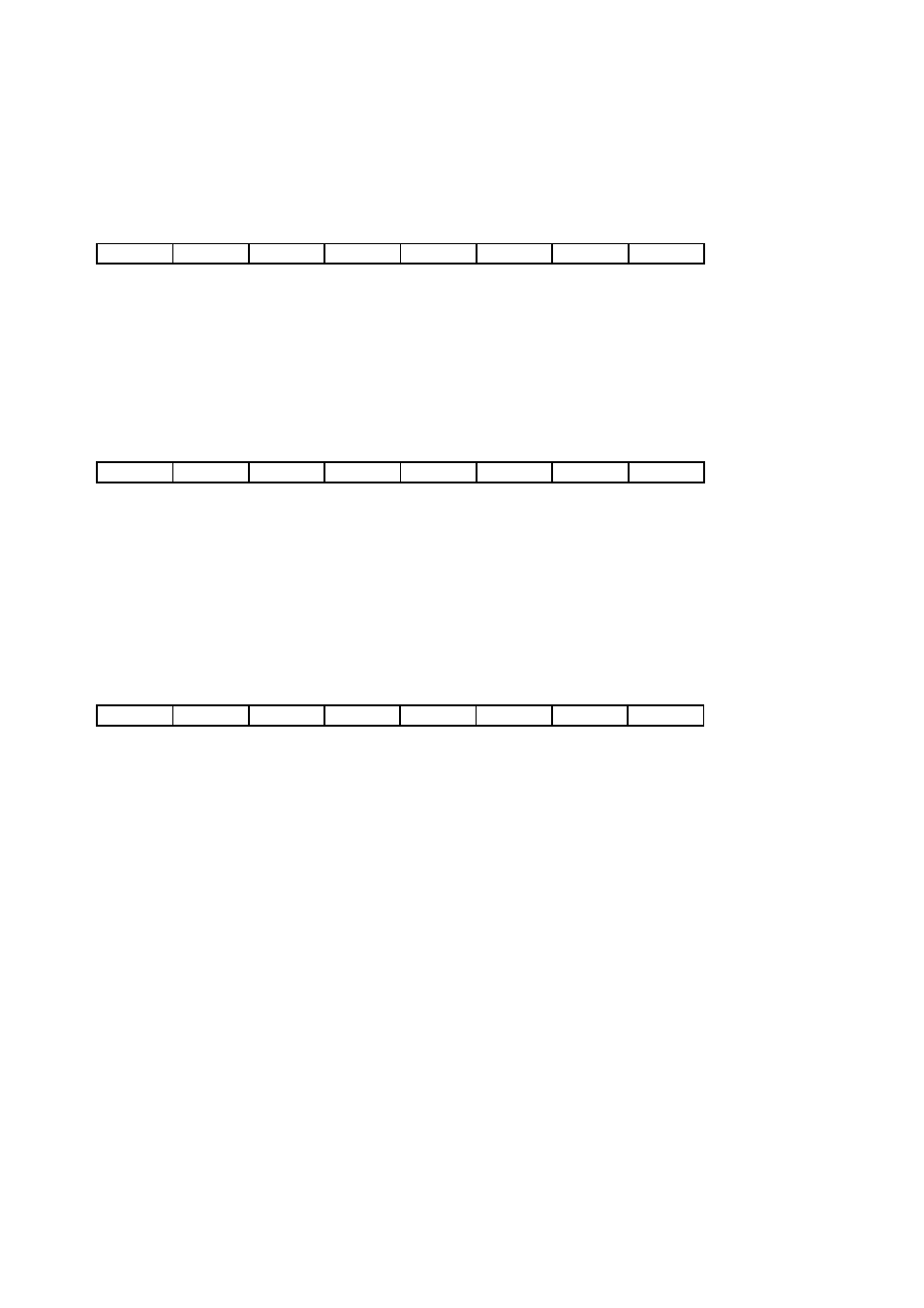
15
14
13
12
11
10
9
8
bit
-
-
-
-
-
-
SEGEN9
SEGEN8
-
-
-
-
-
-
0
0
Initial value
-
-
-
-
-
-
R/W
R/W
Attribute
7
6
5
4
3
2
1
0
bit
SEGEN7
SEGEN6
SEGEN5
SEGEN4
SEGEN3
SEGEN2
SEGEN1
SEGEN0
0
0
0
0
0
0
0
0
Initial value
R/W
R/W
R/W
R/W
R/W
R/W
R/W
R/W
Attribute
7
6
5
4
3
2
1
0
bit
DTCH
–
–
–
COMEN3
COMEN2
COMEN1
COMEN0
0
–
–
–
0
0
0
0
Initial value
R/W
RX/WX
RX/WX
RX/WX
R/W
R/W
R/W
R/W
Attribute