Single read operation timing, Single read/write operation timing – FUJITSU MB91460 SERIES FR60 User Manual
Page 599
583
Chapter 31 External Bus
9.SDRAM/FCRAM Interface Operation
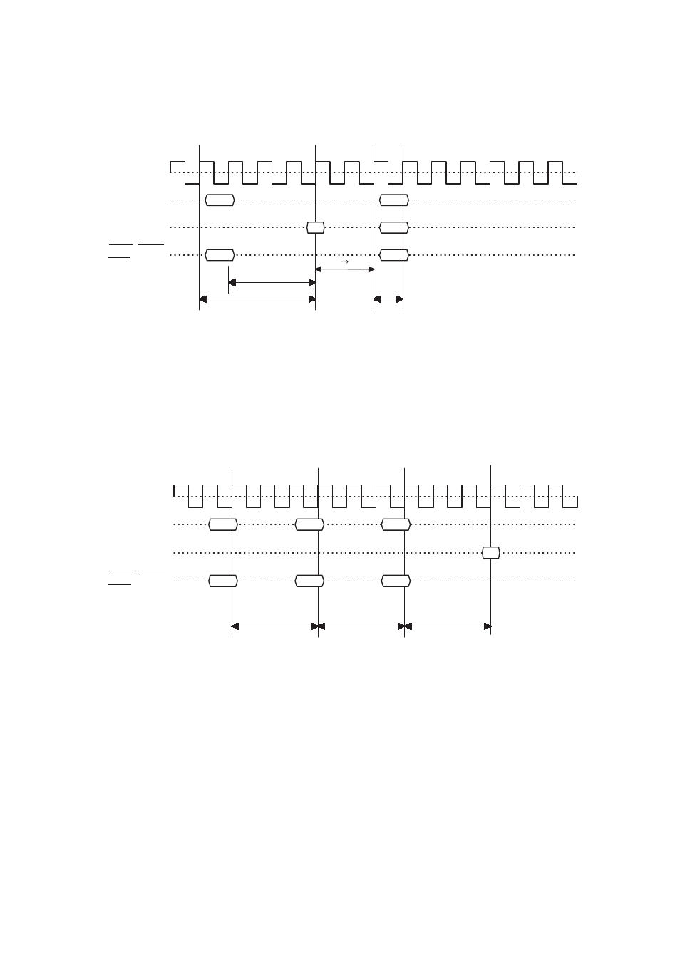
Figure 9-2 Single Read/Write Timing Chart
Set the W07 and W06 bits in the area wait register (AWR) to the read - to - write idle cycle according to the
SDRAM/FCRAM standards.
■
Single Read Operation Timing
shows the operation timings assuming that page misses, CAS latency 3, and no auto - precharge are
set.
Figure 9-3 Single Read Timing Chart
•
When a page miss occurs, a read operation is performed after the PRE charge and ACTV commands are
issued.
•
Set the W01 and W00 bits in the area wait register (AWR) to the RAS precharge cycle (tRP) according to the
SDRAM/FCRAM standards.
•
Set the W14 to W12 bits in the area wait register (AWR) to the RAS - to - CAS delay (tRCD) according to the
SDRAM/FCRAM standards.
■
Single Read/Write Operation Timing
shows the operation timings assuming that CAS latency 1, TYP = 1001
B
, and auto - precharge are set.
MCLK
A
SRAS,SCAS,
SWE
D
READ
#1
#1
#1
WRIT
#1
Cas Latency
Read cycle
Write cycle
Idle cycle
Read
Write
MCLK
A
D
Row
#1
ACT
Cas Latency
#1
READ
RAS precharge cycle
(tRP)
PRE
BA
RAS
→
CAS delay
(tRCD)
SRAS,SCAS,
SWE