2 area configuration registers 0-7 (acr0-7) – FUJITSU MB91460 SERIES FR60 User Manual
Page 529
513
Chapter 31 External Bus
2.External Bus Interface Registers
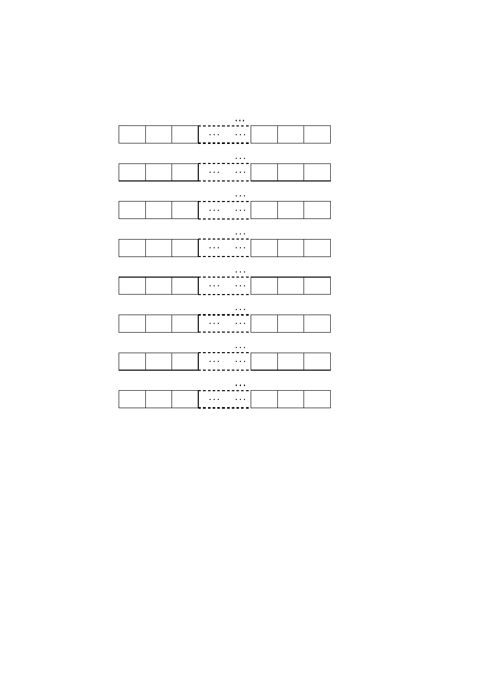
Figure 2-1 Configuration of the Area Select Registers (ASR0-7)
■
Functions of Bits in the Area Select Registers (ASR0-7)
The start address can be set in the high-order 16 bits (bits A31-A16). Each chip select area starts with the
address set in this register and covers the range set by the four bits ASZ3-0 of the ASR0-7 registers.
The boundary of each chip select area obeys the setting of the four bits ASZ3-0 of the ACR0-7 registers. For
example, if an area of 1 MB is set by the four bits ASZ3-0, the low-order four bits of the ASR0-7 registers are
ignored and only bits A31-20 are valid.
The ASR0 register is initialized to 0000
H
by INIT and RST. ASR1-7 are not initialized by INIT and RST, and are
therefore undefined. After starting chip operation, be sure to set the corresponding ASR register before enabling
each chip select area with the CSER register.
2.2 Area Configuration Registers 0-7 (ACR0-7)
This section explains the configuration and functions of area configuration registers 0-7 (ACR0-
7).
■
Configuration of Area Configuration Registers 0-7 (ACR0-7)
The area configuration registers 0-7 (ACR0-7: FArea Configuration Register 0-7) set the function of each chip
Initial value
ASR0
15
14
13
12
2
1
0
INIT
RST
Access
00000640
H
A31
A30
A29
A18
A17
A16
0000
H
0000
H
W/R
ASR1
15
14
13
12
2
1
0
00000644
H
A31
A30
A29
A18
A17
A16
xxxx
H
xxxx
H
W/R
ASR2
15
14
13
12
2
1
0
00000648
H
A31
A30
A29
A18
A17
A16
xxxx
H
xxxx
H
W/R
ASR3
15
14
13
12
2
1
0
0000064C
H
A31
A30
A29
A18
A17
A16
xxxx
H
xxxx
H
W/R
ASR4
15
14
13
12
2
1
0
00000650
H
A31
A30
A29
A18
A17
A16
xxxx
H
xxxx
H
W/R
ASR5
15
14
13
12
2
1
0
00000654
H
A31
A30
A29
A18
A17
A16
xxxx
H
xxxx
H
W/R
ASR6
15
14
13
12
2
1
0
00000658
H
A31
A30
A29
A18
A17
A16
xxxx
H
xxxx
H
W/R
ASR7
15
14
13
12
2
1
0
0000065C
H
A31
A30
A29
A18
A17
A16
xxxx
H
xxxx
H
W/R