2 i/o port block diagram – FUJITSU MB91460 SERIES FR60 User Manual
Page 472
456
Chapter 30 I/O Ports
3.Port Register Settings
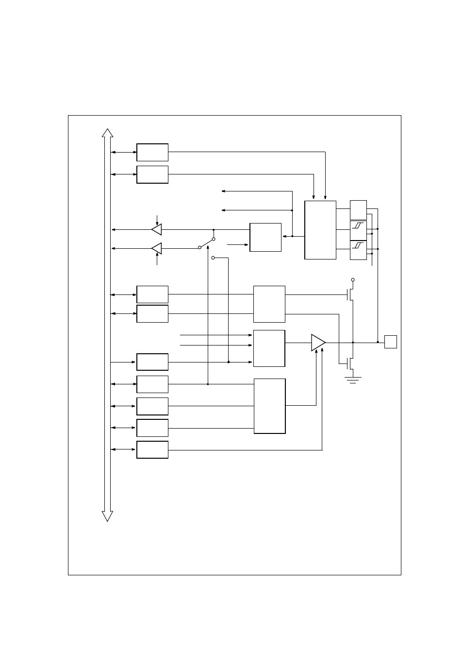
3.2 I/O Port Block Diagram
Port Bus
PDR
DDR
Peripheral inputs
PDRD read
Pin
PDR:
Port Data Register
Address 0x000h + #port (Port00: 0x000h, Port01: 0x001h,...)
PDRD:
Port Data Direct Register
Address = PDR + 0xD00h
DDR:
Data Direction Register
Address = PDR + 0xD40h
PFR:
Port Function Register
Address = PDR + 0xD80h
EPFR:
Extra PFR Port Function Register
Address = PDR + 0xDC0h
optional
PODR: Port Output Drive Register
Address = PDR + 0xE00h
optional
PILR:
Port Input Level selection Register
Address = PDR + 0xE40h
optional
EPILR: Port Input Level selection Register
Address = PDR + 0xE80h
optional
PPER:
Port Pull up/down Enable Register
Address = PDR + 0xEC0h
optional
PPCR:
Port Pull up/down Control Register
Address = PDR + 0xF00h
optional
EPFR
PFR
1. Peripheral output
PPER
EPILR
PPCR
PDR read
Pull Up/
Down
Control
External bus interface inputs
Output
MUX
Port
Direction
Control
CLKP
Out Driver
50 kOhm
50 kOhm
&
&
STOP or
PDRD
2. Peripheral output
1
0
PODR
PILR
&
CMOS
Hysteresis
Automotive
Hysteresis
TTL
GPORTEN