11 dma fly-by transfer (memory -> i/o) – FUJITSU MB91460 SERIES FR60 User Manual
Page 588
572
Chapter 31 External Bus
5.Operation of the Ordinary bus interface
■
Operation Timing for DMA Fly-By Transfer (I/O -> Memory)
"Timing Chart for DMA Fly-By Transfer (I/O -> Memory)" shows the operation timing for (TYP3-
0=0000
B
, AWR=0008
H
, IOWR=51
H
). This timing chart shows a case in which a wait is not set on the memory
side.
Figure 5-10 Timing Chart for DMA Fly-By Transfer (I/O -> Memory)
•
Setting 1 for the HLD bit of the IOWR0-3 registers enables the I/O read cycle to be extended by one cycle.
•
Setting bits IW3-0 of the IOWR0-3 registers enables 0-15 wait cycles to be inserted.
•
If wait is also set on the memory side (AWR15-12 is not 0), the larger value is used as the wait cycle after
comparison with the I/O wait (IW3-0 bits).
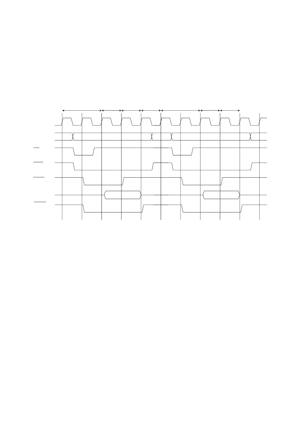
5.11 DMA Fly-By Transfer (Memory -> I/O)
This section shows the operation timing for DMA fly-by transfer (memory -> I/O).
■
Operation Timing for DMA Fly-By Transfer (Memory -> I/O)
"Timing Chart for DMA Fly-By Transfer (Memory -> I/O)" shows the operation timing chart for (TYP3-
0=0000
B
, AWR=0008
H
, IOWR=51
H
). This timing chart shows a case in which a wait is not set on the memory
side.
IORD
Basic cycle
Basic cycle
MCLK
AS
CSn
WRn
D[31:0]
A[31:0]
I/O wait
cycle *
I/O hold
wait *
I/O wait
cycle *
I/O hold
wait *
I/O idle
cycle