FUJITSU MB91460 SERIES FR60 User Manual
Page 548
532
Chapter 31 External Bus
2.External Bus Interface Registers
■
Functions of Bits in the I/O Wait Registers for DMAC (IOWR0-3)
The following explains the functions of the bits in the I/O wait registers for DMAC.
[Bits 31, 23] RYE0,1 (RDY enable 0,1)
These bits set the wait control, using RDY, of channels 0-3 during DMAC fly-by access.
When 1 is set, wait insertion by the RDY pin can be performed during fly-by transfer on the relevant channel.
IOWR and IORD are extended until the RDY pin is enabled. Also, RD/WR0-WR3/WR on the memory side are
extended synchronously. If the chip select area of the fly-by transfer destination is set to RDY-enabled in the
ACR register, wait insertion by the RDY pin can be performed regardless of the RYEn bit of IOWR. When the
chip select area of the fly-by transfer destination is set to RDY-disabled in the ACR register, wait insertion by the
RDY pin can only be performed during fly-by access if the area is set to RDY-enabled by the RYEn bit on the
IOWR side.
[Bits 30,22] HLD0,1 (Hold Wait Control)
These bits control the hold cycle of the read strobe signal on the transfer source access side during DMA fly-
by access.
If 0 is set, the read strobe signal (RD for memory -> I/O and IORD for I/O -> memory) and the write strobe signal
(IOWR for memory -> I/O and WR0-WR3 and WR for I/O -> memory) on the transfer source access side are
output at the same timing.
If 1 is set, the read strobe signal is output one cycle longer than the write strobe signal to secure a hold time for
data at the transfer source access side when sending it to the transfer destination.
[Bits 29, 28, 21, 20] WR01/00, WR11/00 (I/O Idle Wait)
These bits set the number of idle cycles for continuous access during DMA fly-by access.
"Settings
for the Number of I/O Idle Cycles" lists the settings for the number of I/O idle cycles.
If one or more cycles is set as the number of idle cycles, cycles equal to the number specified are inserted after I/
O access during DMA fly-by access. During the idle cycles, all CS and strobe output is negated and the data pin
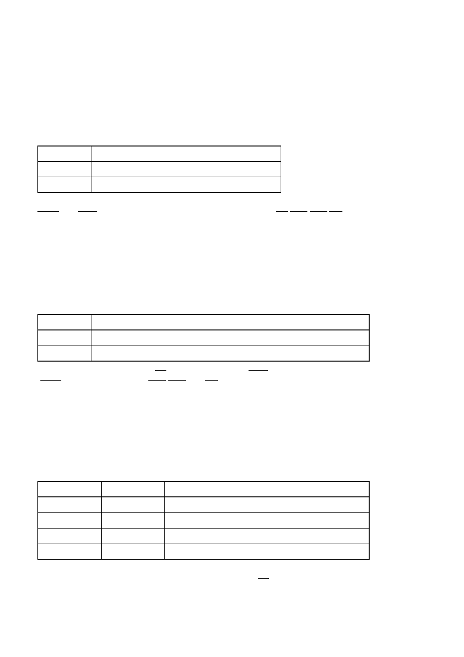
RYEn
RDY function setting
0
Disable RDY input for I/O access.
1
Enable RDY input for I/O access.
HLDn
Hold wait setting
0
Do not insert a hold extension cycle.
1
Insert a hold extension cycle to extend the read cycle by one cycle.
Table 2-22 Settings for the Number of I/O Idle Cycles
WRn1
WRn0
Setting of the number of I/O idle cycles
0
0
0 cycle
0
1
1 cycle
1
0
2 cycles
1
1
3 cycles