Block diagram clock supervisor, Clock supervisor, Internal bus – FUJITSU MB91460 SERIES FR60 User Manual
Page 240: Control logic
224
Chapter 16 Clock Supervisor
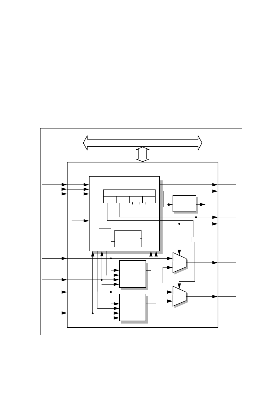
3.Block Diagram Clock Supervisor
3. Block Diagram Clock Supervisor
This section presents a block diagram of the Clock Supervisor. The building blocks of the Clock
Supervisor are:
l Main Clock Supervisor
l Sub-Clock Supervisor
l Control Logic
l RC-Oscillator
■
Block Diagram Clock Supervisor
Figure 3-1 Bock Diagram Clock Supervisor
Remark: SCLK_OUT and MCLK_OUT can be observed using the Clock Monitor Module. SCLK_MISSING and
MCLK_MISSING can be programmed to device specific outputs (see the datasheet of the used device for the infor-
mation which pins are used) by setting OUTE=1.
Internal Bus
Clock Supervisor
Main Clock
Supervisor
MCLK
EN
STBY
RC_CLK
NO_MCLK
Sub-Clock
Supervisor
SCLK
EN
STBY
RC_CLK
NO_SCLK
Control Logic
NO_MCLK
NO_SCLK
SCLK_STBY
SSEN
MCLK_STBY
MSEN
0
1
S
0
1
S
RC_CLK
RC_CLK
RC_CLK
Clock Supervisor Control Register
CSVCR
CLK
RC_CLK
0
1
2
3
4
5
6
7
RCE
SM
MM
OUTE
SCKS
MSVE SSVE SRST
MM
SM
RCE
TO_MCLK
TO_SCLK
Timeout Counter
RC-Oscillator
STBY
RC_CLK
RC_CLK
ERSXO
ERSX
PONR
TB_ST
RC_CLK
EXT_RST_OUT
OUTE
SCLK_MISSING
MCLK_MISSING
MCLK_OUT
SCLK_OUT
EXT_RST
PONR
OSC_STAB
MCLK
MCLK_STBY
SCLK
SCLK_STBY
MUX
MUX
OR
SCKS