FUJITSU MB91460 SERIES FR60 User Manual
Page 534
518
Chapter 31 External Bus
2.External Bus Interface Registers
If an area for which write operations are disabled is accessed for a write operation from the internal bus, the
access is ignored and no external access at all is performed.
Set the WREN bit of areas for which write
operations are not required, such as data areas, to 0.
[Bit 4] LEND (Little ENDian select)
This bit sets the order of bytes of each chip select area as indicated in the following table.
Be sure to set the LEND bit of ACR0 to 0. CS0 supports only the big endian method.
[Bits 3-0] TYP3-0 (TYPe select)
These bits set the access type of each chip select area as indicated in
"Access Type Settings for
Each Chip Select Area".
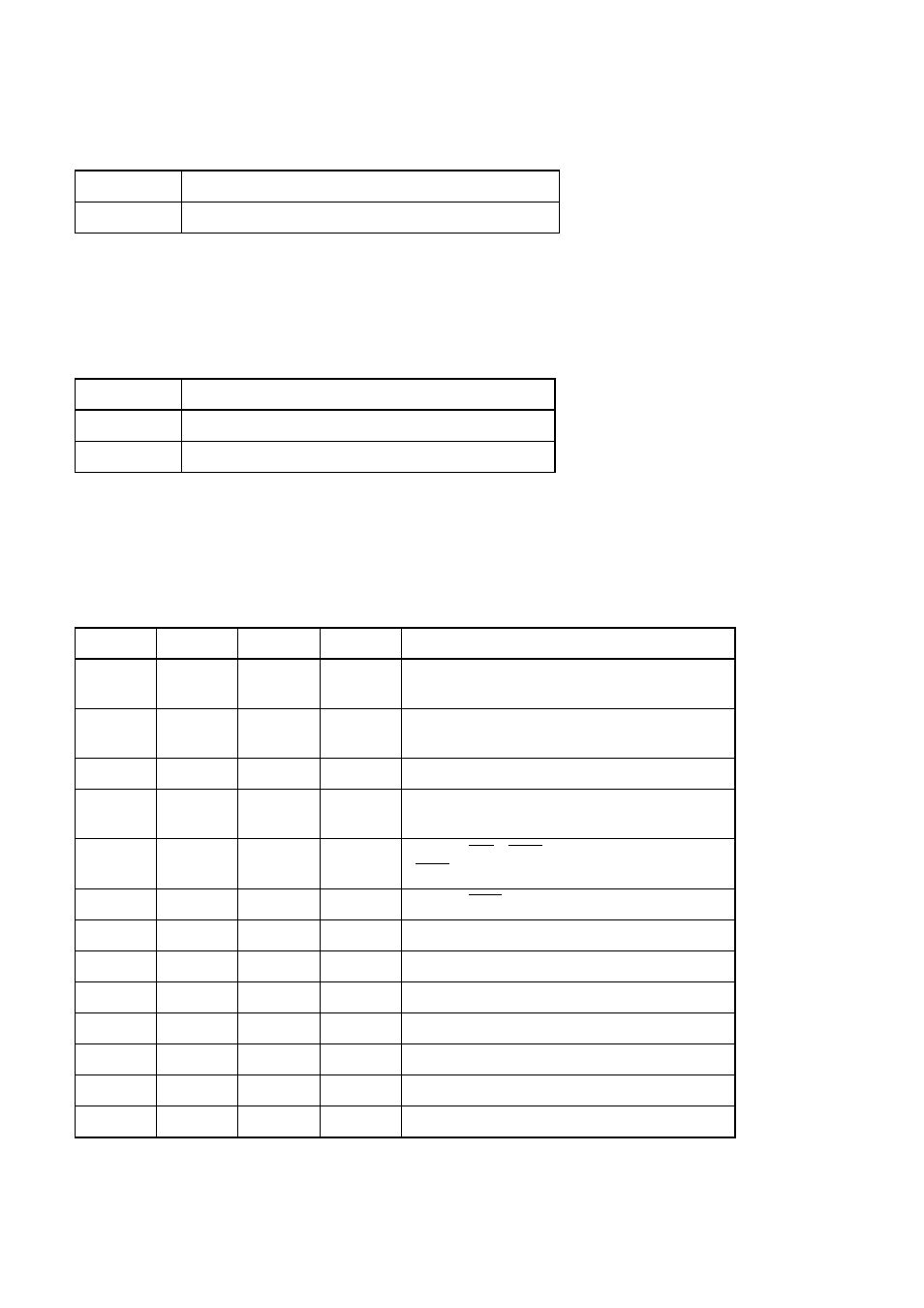
1
Enable write
LEND
Order of bytes
0
Big endian
1
Little endian
Table 2-4 Access Type Settings for Each Chip Select Area
TYP3
TYP2
TYP1
TYP0
Access type
0
0
x
x
Normal access (asynchronous SRAM, I/O,
and single/page/burst-ROM/FLASH)
0
1
x
x
Address data multiplex access (8/16-bit bus
width only)
0
x
x
0
Disable WAIT insertion by the RDY pin.
0
x
x
1
Enable WAIT insertion by the RDY pin
(disabled during bursts).
0
x
0
x
Use the WR0-WR3 pins as write strobes
(WEn is always H).
0
x
1
x
Use the WEn pin as the write strobe.
*1
1
0
0
0
Memory type A: SDRAM/FCRAM
*2
1
0
0
1
Memory type B: FCRAM
*2
1
0
1
0
Setting disabled
1
0
1
1
Setting disabled
1
1
0
0
Setting disabled
1
1
0
1
Setting disabled
1
1
1
0
Setting disabled
WREN
Write enable/disable