5 memory connection example – FUJITSU MB91460 SERIES FR60 User Manual
Page 603
587
Chapter 31 External Bus
9.SDRAM/FCRAM Interface Operation
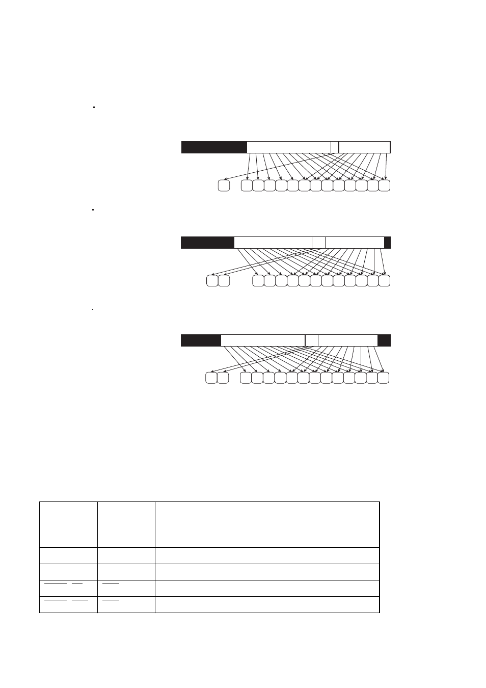
Figure 9-6 Examples of combinations of access addresses and Row/BANK/Column addresses
9.5 Memory Connection Example
This section shows the memory connection example.
Memory Connection Example
The SDRAM/FCRAM interface is connected to SDRAM/FCRAM as shown in Table 4.9 - 1 in principle.
Table 9-1 SDRAM/FCRAM Interface to SDRAM/FCRAM Connection Table
SDRAM/
FCRAM
interface
pin
SDRAM/
FCRAM pin
Remarks
MCLKO
CLK
MCLKE
CKE
SRAS (AS)
RAS
SCAS (BAA)
CAS
BA
COLUMN
0
7
8
9
31
21
22
ROW
BA
COLUMN
0
1110 9
31
23
24
ROW
1
12
BA
COLUMN
0
1110
13
31
25
26
ROW
1
12
2
A8
A9
A10
A11
A12
A14
A15
A7 A6 A5 A4 A3 A2 A1 A0
Access address bit
Access address bit
Access address bit
A8
A9
A10
A11
A14
A15
A7 A6 A5 A4 A3 A2 A1 A0
A8
A9
A10
A11
A12
A14
External address pin
External address pin
External address pin
A7 A6 A5 A4 A3 A2 A1 A0
4M bytes (set ASZ to 0110
B
), 8-bit bus width (set DBW to 00
B
)
256 column (set PSZ to 000
B
), 2 banks (set BANK to 0
B
)
16M bytes (set ASZ to 1000
B
), 16-bit bus width (set DBW to 01
B
)
512 column (set PSZ to 001
B
), 4 banks (set BANK to 1
B
)
64M bytes (set ASZ to 1010
B
), 32-bit bus width (set DBW to 10
B
)
512 column (set PSZ to 001
B
), 4 banks (set BANK to 1
B
)