7 chip select enable register (cser) – FUJITSU MB91460 SERIES FR60 User Manual
Page 550
534
Chapter 31 External Bus
2.External Bus Interface Registers
[Bits 27-24, 19-16, 11-8] IW03-00,IW13-10 (I/O Access Wait)
These bits set the number of auto-wait cycles for I/O access during DMA fly-by access.
"Settings for the Number of I/O Wait Cycles" lists the settings for the number of I/O wait cycles.
Because data is synchronized between the transfer source and transfer destination, the I/O side setting of the
IWnn bits and the wait setting for the fly-by transfer destination (such as memory), whichever is larger, is used as
the number of wait cycles to be inserted. Consequently, more wait cycles than specified by the IWnn bits may be
inserted.
2.7 Chip Select Enable Register (CSER)
Because data is synchronized between the transfer source and transfer destination, the I/O side
setting of the IWnn bits and the wait setting for the fly-by transfer destination (such as memory),
whichever is larger, is used as the number of wait cycles to be inserted. Consequently, more
wait cycles than specified by the IWnn bits may be inserted.
■
Configuration of the Chip Select Enable Register (CSER)
The chip select enable register (CSER: Chip Select Enable register) enables and disables each chip select area.
"Configuration of the Chip Select Enable Register (CSER)" shows the configuration of the chip select
enable register (CSER).
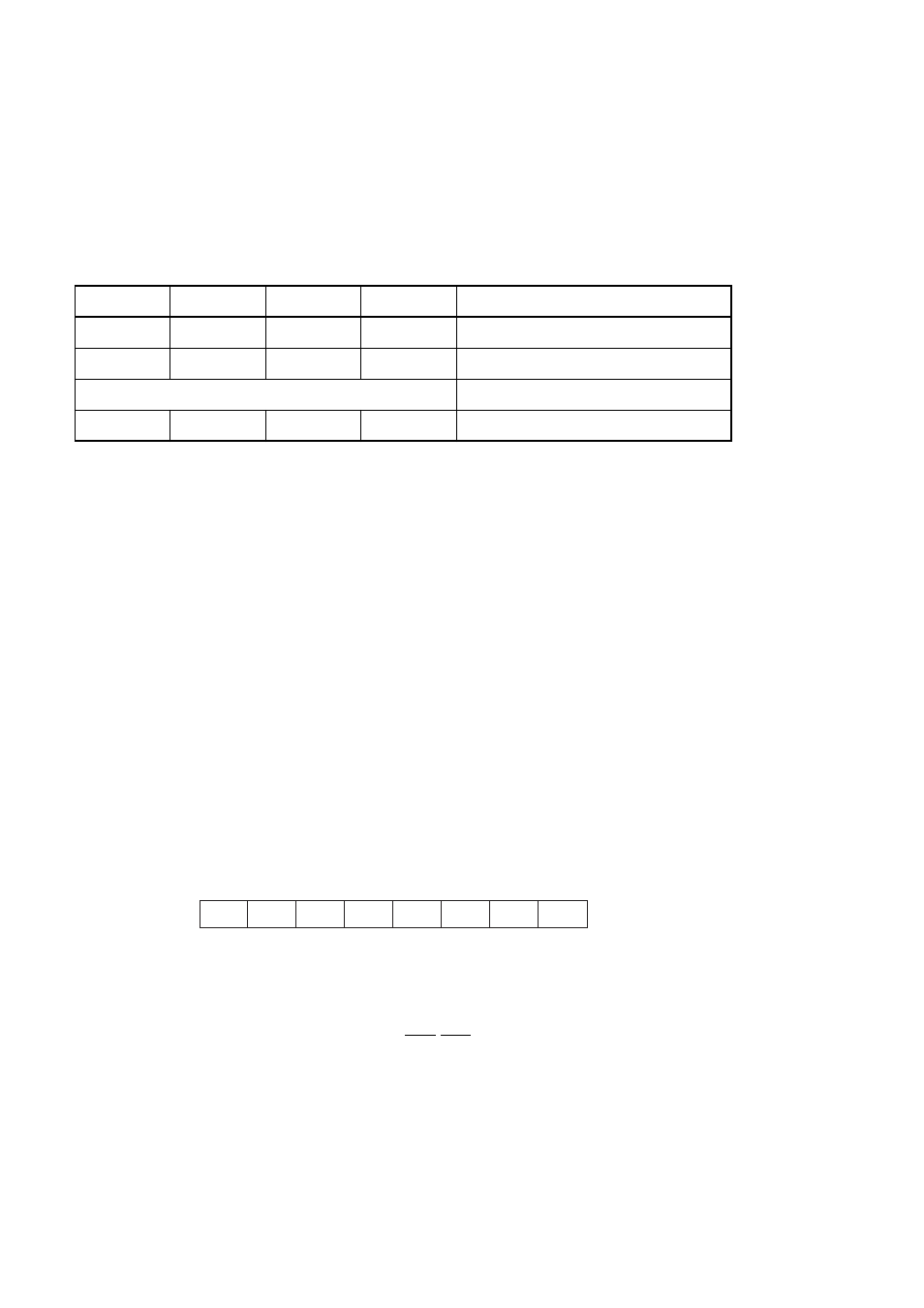
Figure 2-7 Configuration of the Chip Select Enable Register (CSER)
■
Functions of Bits in the Chip Select Enable Register (CSER)
The following explains the functions of the bits in the chip select enable register (CSER).
[Bits 31-24] CSE7-0 (Chip Select Enable 0-7)
These bits are the chip select enable bits for CS0-CS7.
The initial value is 00000001
B
, which enables only the CS0 area.
When 1 is written, a chip select area operates according to the settings of ASR0-7, ACR0-7, and AWR0-7.
Table 2-23 Settings for the Number of I/O Wait Cycles
IWn3
IWn2
IWn1
IWn0
Number of I/O wait cycles
0
0
0
0
0 cycle
0
0
0
1
1 cycle
...
...
1
1
1
1
15 cycle
31 30 29 28 27 26 25 24
00000680
H
CSE7 CSE6 CSE5 CSE4 CSE3 CSE2 CSE1 CSE0
00000001
B
00000001
B
R/W
Initial value
INIT RST Access