Address/data multiplex interface – FUJITSU MB91460 SERIES FR60 User Manual
Page 592
576
Chapter 31 External Bus
7.Address/data Multiplex Interface
7. Address/data Multiplex Interface
This section explains the following three cases of operation of the address/data multiplex inter-
face:
• Without external wait
• With external wait
• CSn -> RD/WRn setup
■
Without External Wait
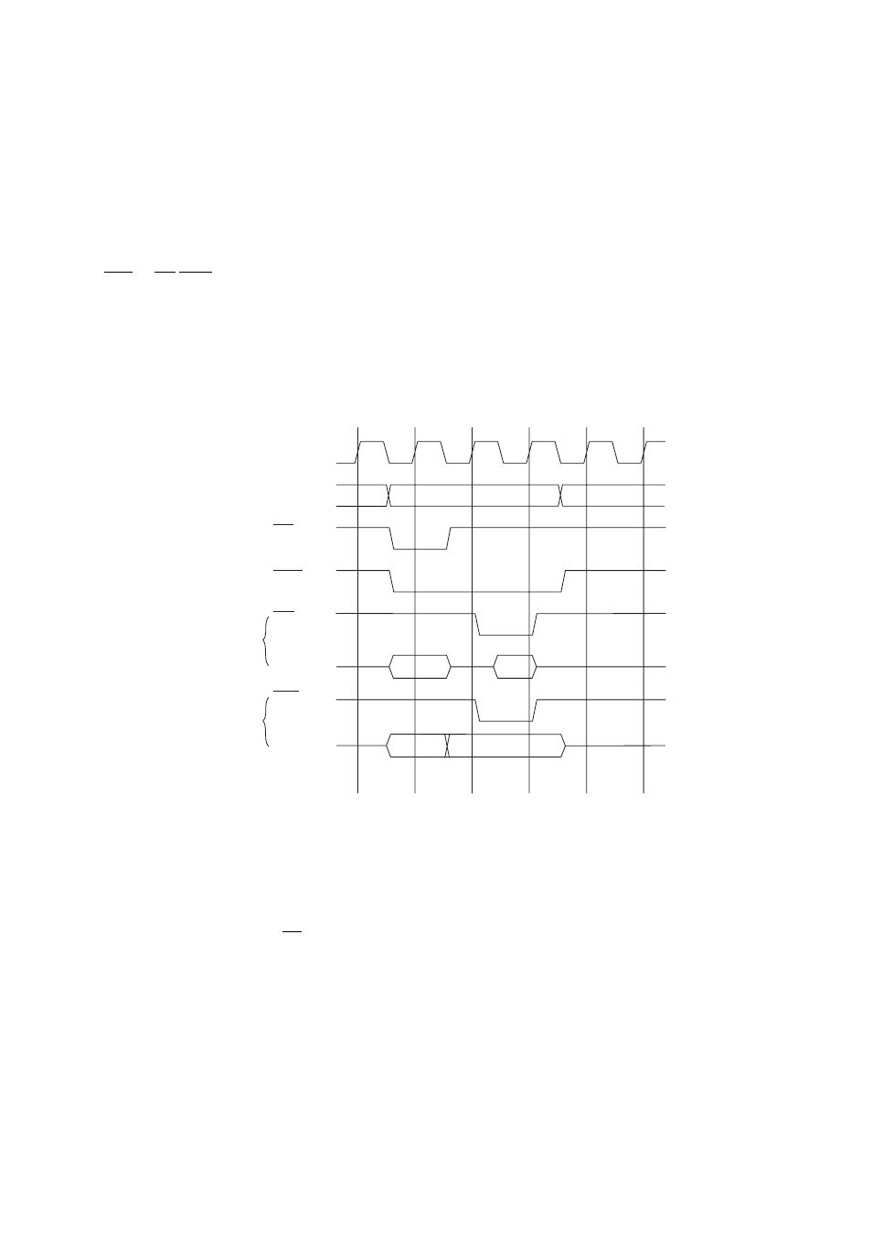
"Timing Chart for the Address/Data Multiplex Interface (without External Wait)" shows the operation
timing chart for (TYP3-0=0100
B
, AWR=0008
H
).
Figure 7-1 Timing Chart for the Address/Data Multiplex Interface (without External Wait)
•
Making a setting such as TYP3-0=01xx
B
in the ACR register enables the address/data multiplex interface to
be set.
•
If the address/data multiplex interface is set, set 8 bits or 16 bits for the data bus width (DBW1-0 bits).
•
In the address/data multiplex interface, the total of 3 cycles of 2 address output cycles + 1 data cycle becomes
the basic number of access cycles.
•
In the address output cycles, AS is asserted as the output address latch signal.
•
As with a normal interface, the address indicating the start of access is output to A31-0 during the time division
bus cycle. Use this address if you want to use an address more than 8/16 bits in the address/data multiplex
interface.
address[31:0]
address[15:0]
data[15:0]
address[15:0]
data[15:0]
MCLK
AS
CSn
RD
A[31:0]
D[31:16]
D[31:0]
WR
WRITE
READ