8 cache enable register (cher) – FUJITSU MB91460 SERIES FR60 User Manual
Page 551
535
Chapter 31 External Bus
2.External Bus Interface Registers
Before setting this register, be sure to make all settings required for the corresponding chip select areas.
" CSn Corresponding to the Chip Select Enable Bits" lists the corresponding CSn for the chip select
enable bits.
2.8 Cache Enable Register (CHER)
This section explains the configuration and functions of the cache enable register (CHER).
■
Configuration of the Cache Enable Register (CHER)
The cache enable register (CHER: CacHe Enable Register) controls the transfer of data read from each chip
select area.
"Configuration of the Cache Enable Register (CHER)" shows the configuration of the cache enable
register (CHER).
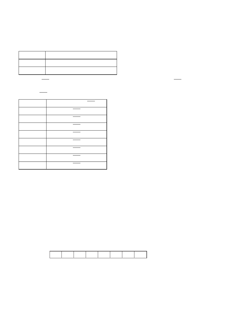
Figure 2-8 Configuration of the Cache Enable Register (CHER)
■
Functions of Bits in the Cache Enable Register (CHER)
The following explains the functions of the bits in the cache enable register (CHER).
CSE7-0
Area control
0
Disable
1
Enable
Table 2-24 CSn Corresponding to the Chip Select Enable Bits
CSE bit
Corresponding CSn
Bit 24: CSE0
CS0
Bit 25: CSE1
CS1
Bit 26: CSE2
CS2
Bit 27: CSE3
CS3
Bit 28: CSE4
CS4
Bit 29: CSE5
CS5
Bit 30: CSE6
CS6
Bit 31: CSE7
CS7
23 22 21 20 19 18 17 16
00000681
H
CHE7 CHE6 CHE5 CHE4 CHE3 CHE2 CHE1 CHE0 11111111
B
111111111
B
R/W
Initial value
INIT RST Access