2 dram control register (dcr), Dram control register (dcr) -24, 2 dram control register (dcr) – Motorola DSP56301 User Manual
Page 98: And the refresh access generation, Before

Bus Interface Unit (BIU) Registers
4
-24
DSP56301 User’s Manual
4.6.2
DRAM Control Register (DCR)
The DRAM controller is an efficient interface to dynamic RAM devices in both random
read/write cycles and Fast Access mode (Page mode). An on-chip DRAM controller controls
the page hit circuit, the address multiplexing (row address and column address), the control
signal generation (
CAS
and
RAS
) and the refresh access generation (
CAS
before
RAS
) for a
variety of DRAM module sizes and access times. The on-chip DRAM controller
configuration is determined by the DRAM Control Register (DCR). The DRAM Control
Register (DCR) is a 24-bit read/write register that controls and configures the external DRAM
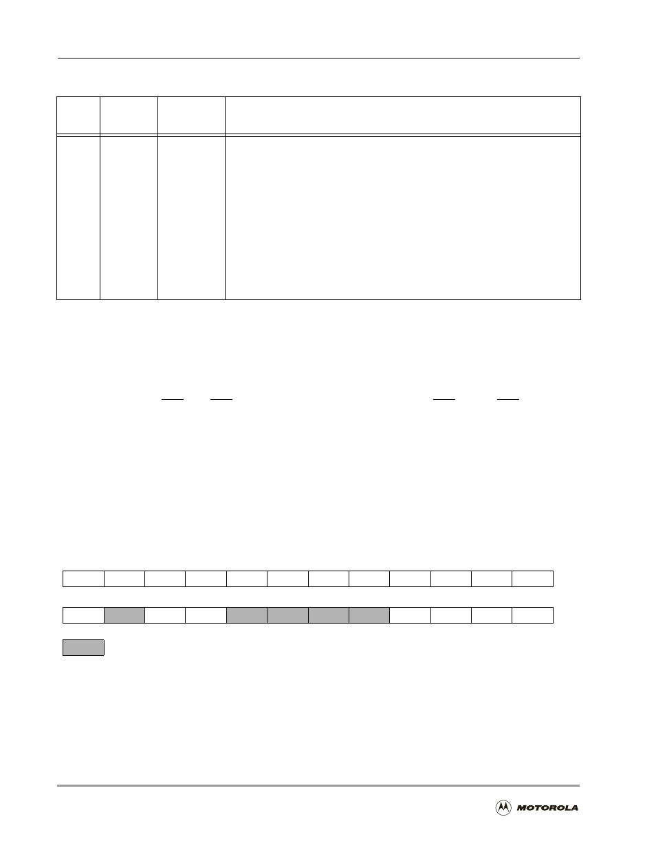
accesses. The DCR bits are shown in Figure 4-7.
Note:
To prevent improper device operation, you must guarantee that all the DCR bits
except BSTR are not changed during a DRAM access.
Figure 4-7. DRAM Control Register (DCR)
4–0
BA0W[4–0]
11111
(31 wait
states)
Bus Area 0 Wait State Control
Defines the number of wait states (one through 31) inserted in each external
SRAM access to Area 0 (DRAM accesses are not affected by these bits). Area 0 is
the area defined by AAR0.
Note:
Do not program the value of these bits as zero, since SRAM memory
access requires at least one wait state.
When selecting four through seven wait states, one additional wait state is inserted
at the end of the access. When selecting eight or more wait states, two additional
wait states are inserted at the end of the access. These trailing wait states increase
the data hold time and the memory release time and do not increase the memory
access time.
Table 4-9. Bus Control Register (BCR) Bit Definitions (Continued)
Bit
Number
Bit Name
Reset Value
Description
23
22
21
20
19
18
17
16
15
14
13
12
BRP
BRF7
BRF6
BRF5
BRF4
BRF3
BRF2
BRF1
BRF0
BSTR
BREN
BME
11
10
9
8
7
6
5
4
3
2
1
0
BPLE
BPS1
BPS0
BRW1
BRW0
BCW1
BCW0
Reserved bit. Read as zero; write to zero for future compatibility
