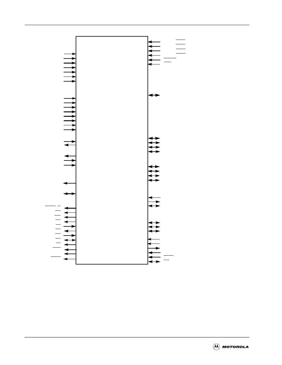
Signals identified by functional group -2, Figure 2-1 and, Figure 2-1. signals identified by functional group – Motorola DSP56301 User Manual
Page 32

2
-2
DSP56301 User’s Manual
Figure 2-1. Signals Identified by Functional Group
DSP56301
24
24
External
Address Bus
External
Data Bus
External
Bus
Control
Extended Synchronous
Serial Interface Port 0
(ESSI0)
2
Timers
3
PLL
JTAG/OnCE
Port
Power Inputs:
PLL
Internal Logic
Address Bus
Data Bus
Bus Control
HI32
ESSI/SCI/Timer
A[0–23]
D[0–23]
AA[0–3]/
RAS[0–3]
RD
WR
BS
TA
BR
BG
BB
BL
CAS
BCLK
BCLK
TCK
TDI
TDO
TMS
TRST
DE
CLKOUT
PCAP
PINIT
V
CCP
V
CCQ
V
CCA
V
CCD
V
CCC
V
CCH
V
CCS
4
Serial
Communications
Interface (SCI) Port
2
4
2
2
Grounds:
PLL
PLL
Internal Logic
Address Bus
Data Bus
Bus Control
HI32
ESSI/SCI/Timer
GND
P
GND
1P
GND
Q
GND
A
GND
D
GND
N
GND
H
GND
S
4
6
4
2
Interrupt/
Mode
Control
MODA/IRQA
MODB/IRQB
MODC/IRQC
MODD/IRQD
RESET
Host
Interface
(HI32) Port
1
PCI Bus
RXD
TXD
SCLK
SC0[0–2]
SCK0
SRD0
STD0
TIO0
TIO1
TIO2
52
3
6
2
EXTAL
XTAL
Clock
Extended
Synchronous Serial
Interface Port 1
(ESSI1)
2
SC1[0–2]
SCK1
SRD1
STD1
3
Universal
Bus
Port B
GPIO
Port E GPIO
PE0
PE1
PE2
Port C GPIO
PC[0–2]
PC3
PC4
PC5
Port D GPIO
PD[0–2]
PD3
PD4
PD5
Timer GPIO
TIO0
TIO1
TIO2
Port A
4
6
6
See Figure 2-2 for a listing of the Host
Interface/Port B Signals
Notes: 1.
The HI32 port supports PCI and non-PCI bus configurations. Twenty-four of these HI32 signals can
also be configured alternately as GPIO signals (PB[0–23]).
2.
The ESSI0, ESSI1, and SCI signals are multiplexed with the Port C GPIO signals (PC[0–5]), Port D
GPIO signals (PD[0–5]), and Port E GPIO signals (PE[0–2]), respectively.
3.
TIO[0–2] can be configured as GPIO signals.
NMI
