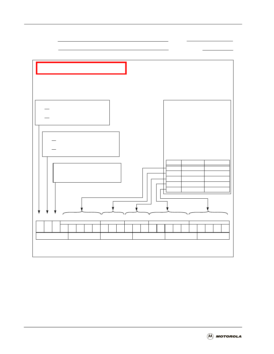
Figure b-6, Bus control register (bcr), Bus interface unit – Motorola DSP56301 User Manual
Page 330: Figure b-6. bus control register (bcr)

Programming Sheets
B
-18
DSP56301 User’s Manual
Figure B-6. Bus Control Register (BCR)
Bus Interface Unit
Bus Control Register (BCR)
Reset = $1FFFFF
Bus State, Bit 21
0 = DSP is not bus master
Area 0 Wait Control, Bits 4– 0
Default Area Wait Control, Bits 20–16
1 = DSP is bus master
Bus Lock Hold, Bit 22
0 = BL pin is asserted only for attempted read-
1 = BL pin is always asserted
Area 3 Wait Control, Bits 15–13
Area 2 Wait Control, Bits 12–10
write modify external access
Bus Request Hold, Bit 23
0 = BR pin is asserted only for attempted
1 = BR pin is always asserted
or pending access
NOTE: All BCR bits are read/write control bits.
These read/write control bits define
the number of wait states inserted
into each external SRAM access to
the designated area. The value of
these bits should not be programmed
as zero.
Area 1 Wait Control, Bits 9–5
Application:
Date:
Programmer:
Sheet 1 of 3
Bits
Bit Name
# of Wait States
20–16
BDFW[4–0]
0–31
15–13
BA3W[2–0]
0–7
12–10
BA2W[2–0]
0–7
9–5
BA1W[4–0]
0–31
4–0
BA0W[4–0]
0–31
15 14 13 12 11 10
9
8
7
6
5
4
3
2
1
0
19 18 17 16
23 22 21 20
BRH
BLH
BBS
BDFW[4–0]
BA3W[2–0]
BA2W[2–0]
BA1W[4–0]
BA0W[4–0]
X:$FFFFFB Read/Write
