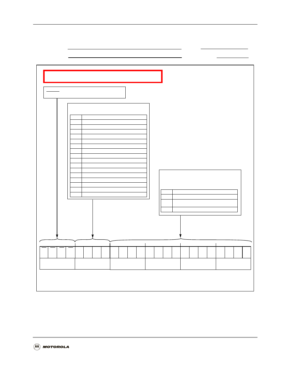
B-13, Figure b-13, Dsp pci address register (dpar) – Motorola DSP56301 User Manual
Page 337: Host processor (hi32), Figure b-13. dsp pci address register (dpar), Programming sheets, B-25, Programming reference, Application: date: programmer

Programming Sheets
Programming Reference
B
-25
Figure B-13. DSP PCI Address Register (DPAR)
DSP PCI Address Register (DPAR)
Reset = $000000
15 14 13 12 11 10
9
8
7
6
5
4
3
2
1
0
AR5
AR2
AR1
19 18 17 16
23 22 21 20
AR14
C3
C2
BE0
BE1
AR4
C0
AR15
AR12
AR9
AR7
Note: All bits work only in PCI mode (DCTR[HM] = $1). You can write to the DPAR only if MARQ is set.
Address: X:FFFFC7 Read/Write
BE3
BE2
C1
AR13
AR11
AR10
AR8
AR6
AR3
AR0
PCI Byte Enables, Bits 23–20
BE[3–0] enable byte lanes 3–0, respectively.
Host Processor (HI32)
Application:
Date:
Programmer:
Sheet 4 of 10
PCI Bus Command, Bits 19–16
C[3–0]
Command Type
0000
Illegal
0001
Illegal
0010
I/O Read
0011
I/O Write
0100
Illegal
0101
Illegal
0110
Memory Read
0111
Memory Write
1000
Illegal
1001
Illegal
1010
Configuration Read
1011
Configuration Write
1100
Memory Read Multiple
1101
Illegal
1110
Memory Read Line
1111
Memory Write and Invalidate
Defines PCI bus commands, as follows:
DSP PCI Transaction Address (Low)
AR[1–0]
Burst Order
00
Linear incrementing
01
PCI Cache line toggle mode (DSP software arranges
data.
1x
Reserved
The two least significant bytes of the 32-bit
PCI transaction address. In addition, the
lowest two bits have the following meaning:
