Motorola DSP56301 User Manual
Page 100

Bus Interface Unit (BIU) Registers
4
-26
DSP56301 User’s Manual
11
BPLE
0
Bus Page Logic Enable
Enables/disables the in-page identifying logic. When BPLE is set, it enables the page
logic (the page size is defined by BPS[1–0] bits). Each in-page identification causes the
DRAM controller to drive only the column address (and the associated CAS signal).
When BPLE is cleared, the page logic is disabled, and the DRAM controller always
accesses the external DRAM in out-of-page accesses (for example, row address with
RAS assertion and then column address with CAS assertion). This mode is useful for
low power dissipation. Only one in-page identifying logic exists. Therefore, during
switches from one DRAM external bank to another DRAM bank (the DRAM external
banks are defined by the access type bits in the AARs, different external banks are
accessed through different AA/RAS pins), a page fault occurs.
10
0
Reserved. Write to zero for future compatibility.
9–8
BPS[1–0]
0
Bus DRAM Page Size
Defines the size of the external DRAM page and thus the number of the column
address bits. The internal page mechanism works according to these bits only if the
page logic is enabled (by the BPLE bit). The four combinations of BPS[1–0] enable the
use of many DRAM sizes (1 M bit, 4 M bit, 16 M bit, and 64 M bit). The encoding of
BPS[1–0] is:
n
00 = 9-bit column width, 512 words
n
01 = 10-bit column width, 1 K words
n
10 = 11-bit column width, 2 K words
n
11 = 12-bit column width, 4 K words
When the row address is driven, all 24 bits of the external address bus are driven [for
example, if BPS[1–0] = 01, when driving the row address, the 14 MSBs of the internal
address (XAB, YAB, PAB, or DAB) are driven on address lines A[0–13], and the
address lines A[14–23] are driven with the 10 MSBs of the internal address. This
method enables the use of different DRAMs with the same page size.
7–4
0
Reserved. Write to zero for future compatibility.
3–2
BRW[1–0]
0
Bus Row Out-of-page Wait States
Defines the number of wait states that should be inserted into each DRAM out-of-page
access. The encoding of BRW[1–0] is:
n
00 = 4 wait states for each out-of-page access
n
01 = 8 wait states for each out-of-page access
n
10 = 11 wait states for each out-of-page access
n
11 = 15 wait states for each out-of-page access
1–0
BCW[1–0]
0
Bus Column In-Page Wait State
Defines the number of wait states to insert for each DRAM in-page access. The
encoding of BCW[1–0] is:
n
00 = 1 wait state for each in-page access
n
01 = 2 wait states for each in-page access
n
10 = 3 wait states for each in-page access
n
11 = 4 wait states for each in-page access
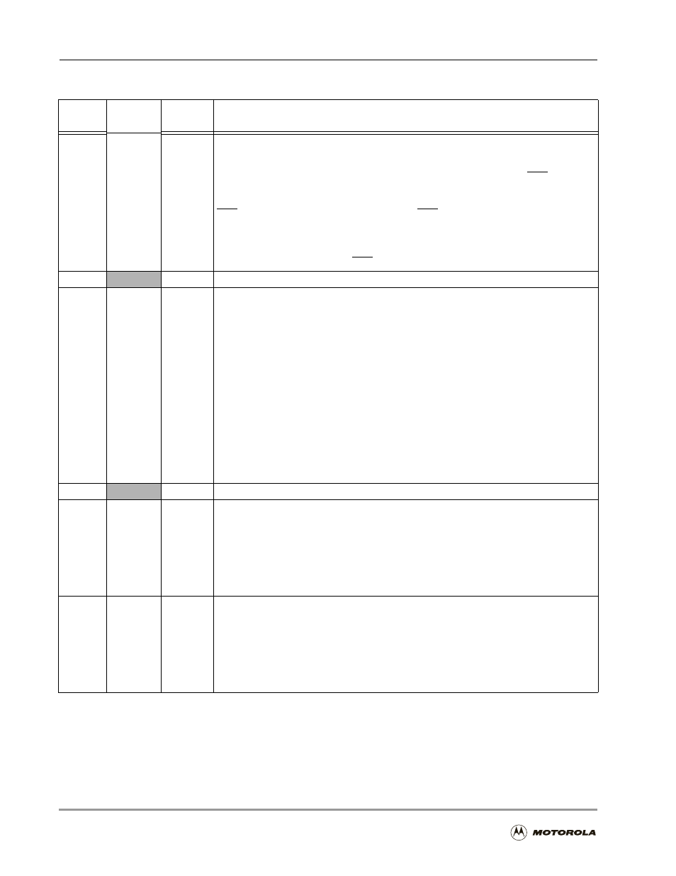
Table 4-10. DRAM Control Register (DCR) Bit Definitions (Continued)
Bit
Number
Bit Name
Reset
Value
Description
