2 essi data and control signals, 1 serial transmit data signal (std), 2 serial receive data signal (srd) – Motorola DSP56301 User Manual
Page 201: 3 serial clock (sck), Essi data and control signals -3, Serial transmit data signal (std) -3, Serial receive data signal (srd) -3, Serial clock (sck) -3, Essi clock sources -3, 2 essi data and control signals

ESSI Data and Control Signals
Enhanced Synchronous Serial Interface (ESSI)
7
-3
7.2
ESSI Data and Control Signals
Three to six signals are required for ESSI operation, depending on the operating mode
selected. The serial transmit data (
STD
) signal and serial control (
SC0
and
SC1
) signals are
fully synchronized to the clock if they are programmed as transmit-data signals.
7.2.1
Serial Transmit Data Signal (STD)
The
STD
signal transmits data from the serial transmit shift register.
STD
is an output when
data is transmitted from the TX0 shift register. With an internally-generated bit clock, the
STD
signal becomes a high impedance output signal for a full clock period after the last data bit is
transmitted if another data word does not follow immediately. If sequential data words are
transmitted, the
STD
signal does not assume a high-impedance state. The
STD
signal can be
programmed as a GPIO signal (
P5
) when the ESSI
STD
function is not in use.
7.2.2
Serial Receive Data Signal (SRD)
SRD
receives serial data and transfers the data to the receive shift register.
SRD
can be
programmed as a GPIO signal (
P4
) when the
SRD
function is not in use.
7.2.3
Serial Clock (SCK)
SCK
is a bidirectional signal providing the serial bit rate clock for the ESSI interface. The
signal is a clock input or output used by all the enabled transmitters and receivers in
Synchronous modes or by all the enabled transmitters in Asynchronous modes. See Table 7-1
for details.
SCK
can be programmed as a GPIO signal (
P3
) when not used as the ESSI clock.
Note:
Although an external serial clock can be independent of and asynchronous to the
DSP system clock, the external ESSI clock frequency must not exceed F
core
/3, and
each ESSI phase must exceed the minimum of 1.5
CLKOUT
cycles. The internally
sourced ESSI clock frequency must not exceed F
core
/4.
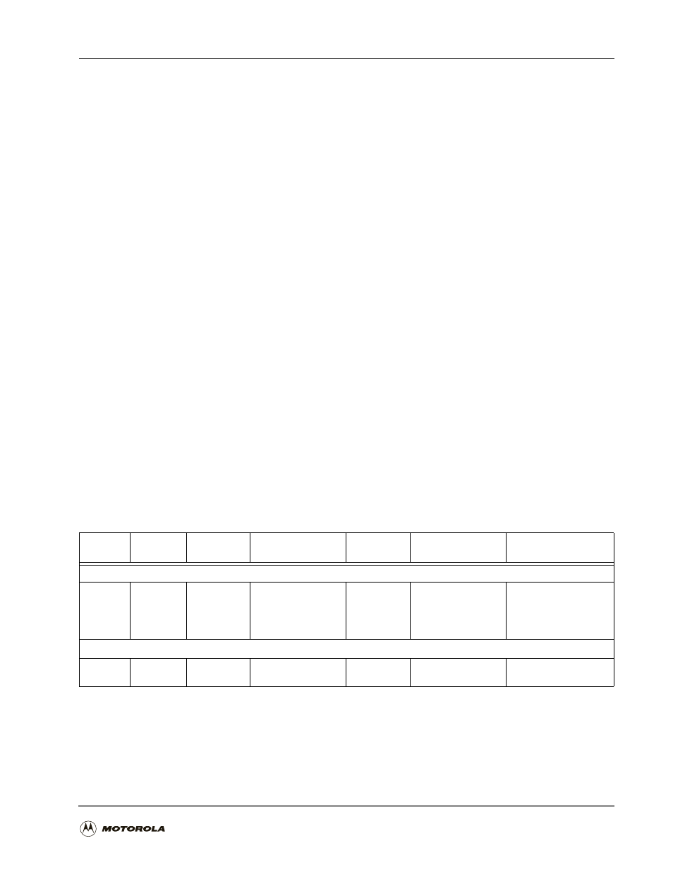
Table 7-1. ESSI Clock Sources
SYN
SCKD
SCD0
RX Clock Source
RX Clock
Out
TX Clock Source
TX Clock Out
Asynchronous
0
0
0
EXT, SC0
—
EXT, SCK
—
0
0
1
INT
SC0
EXT, SCK
—
0
1
0
EXT, SC0
—
INT
SCK
0
1
1
INT
SC0
INT
SCK
Synchronous
1
0
0/1
EXT, SCK
—
EXT, SCK
—
1
1
0/1
INT
SCK
INT
SCK
