7 gpio signals and registers, 1 port e control register (pcre), Gpio signals and registers -24 – Motorola DSP56301 User Manual
Page 260: Port e control register (pcre) -24, Port e control register (pcre x:$ffff9f) -24, 7 gpio signals and registers, 1 port e control register (pcre)

GPIO Signals and Registers
8
-24
DSP56301 User’s Manual
prevent overruns unless transmit interrupts are enabled. Either STX or STXA is usually
written as part of the interrupt service routine. An interrupt is generated only if TDRE is set.
The transmit shift register is indirectly visible via the SSR[TRNE] bit.
In Synchronous mode, data is synchronized with the transmit clock. That clock can have
either an internal or external source, as defined by the TCM bit in the SCCR. The length and
format of the serial word is defined by the WDS0, WDS1, and WDS2 control bits in the SCR.
In Asynchronous mode, the start bit, the eight data bits (with the LSB first if SSFTD = 0 and
the MSB first if SSFTD = 1), the address/data indicator bit or parity bit, and the stop bit are
transmitted in that order. The data to be transmitted can be written to any one of the three STX
addresses. If SCKP is set and SSHTD is set, SCI Synchronous mode is equivalent to the SSI
operation in 8-bit data on-demand mode.
Note:
When data is written to a peripheral device, there is a two-cycle pipeline delay until
any status bits affected by this operation are updated. If you read any of those status
bits within the next two cycles, the bit does not reflect its current status. For details
see the DSP56300 Family Manual.
8.7
GPIO Signals and Registers
Three registers control the GPIO functionality of the SCI pins: Port E control register
(PCRE), Port E direction register (PRRE) and Port E data register (PDRE).
8.7.1
Port E Control Register (PCRE)
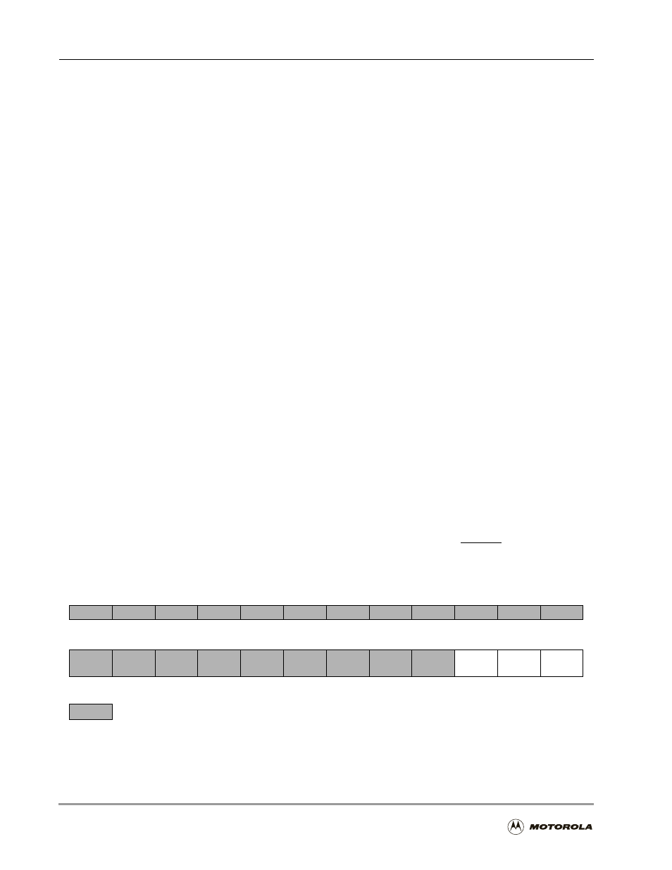
The read/write PCRE controls the functionality of SCI GPIO signals. Each of the PCRE[2–0]
bits controls the functionality of the corresponding port signal. When a PCRE[i] bit is set, the
corresponding port signal is configured as an SCI signal. When a PC[i] bit is cleared, the
corresponding port signal is configured as a GPIO signal. A hardware
RESET
signal or a
software RESET instruction clears all PCRE bits.
23
22
21
20
19
18
17
16
15
14
13
12
11
10
9
8
7
6
5
4
3
2
1
0
PE2/
SCLK
PE1/
TXD
PE0/
RXD
Note:
For bits 2–0, a 0 selects PEn as the signal and a 1 selects the specified SCI signal.
= Reserved. Read as zero. Write to zero for future compatibility.
Figure 8-8. Port E Control Register (PCRE X:$FFFF9F)
