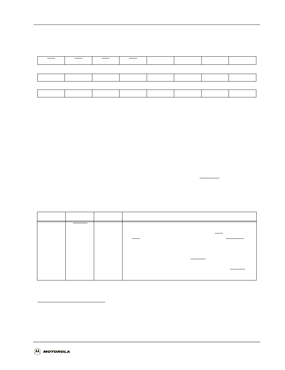
4 dsp pci address register (dpar), Dsp pci address register (dpar) -33, 4 dsp pci address register (dpar) – Motorola DSP56301 User Manual
Page 151: When the hi32 can complete the first data phase, Pins and the bus command is driven to the

HI32 DSP-Side Programming Model
Host Interface (HI32)
6
-33
6.7.4
DSP PCI Address Register (DPAR)
A 24-bit read/write register by which the DSP56300 core generates the two least significant
bytes of the 32-bit PCI transaction address, the PCI bus command and the PCI bus byte
enables. The host processor cannot access DPAR. The two most significant bytes of the PCI
transaction address are located in the DSP PCI Master Control register (DPMC, see Section
6.7.3, DSP PCI Master Control Register (DPMC), on page 6-30).
When the DSP56300 core writes to DPAR in PCI mode (DCTR[HM]
=
$1), DPSR[MARQ]
is cleared.
1
When the HI32 can complete the first data phase,
2
ownership of the PCI bus is
requested. When the request is granted, the address (from the DPMC and the DPAR) is driven
to the
HAD[31
–
0]
pins and the bus command is driven to the
HC[3–0]
/
HBE[3–0]
pins during the
PCI address phase. The DPAR can be written only if MARQ is set.
23
22
21
20
19
18
17
16
BE3
BE2
BE1
BE0
C3
C2
C1
C0
15
14
13
12
11
10
9
8
AR15
AR14
AR13
AR12
AR11
AR10
AR9
AR8
7
6
5
4
3
2
1
0
AR7
AR6
AR5
AR4
AR3
AR2
AR1
AR0
Figure 6-8. DSP PCI Address Register (DPAR)
1. DPSR[MARQ] is the PCI Master Address Request bit in the DSP PCI Status Register. This bit indicates that
the HI32 is currently not the initiator of a PCI transaction and the DPAR can be written with the address of the
next transaction.
2. That is, in a write transaction, the DSP-to-host data path is not empty; in a read transaction, the host-to-DSP
data path is not full.
Table 6-13. DSP PCI Address Register (DPAR) Bit Definitions
Bit Number
Bit Name
Reset Value
Description
23–20
BE[3–0]
0
PCI Byte Enables
Determine which byte lanes carry meaningful data in PCI mode
(DCTR[HM]
=
$1) when the HI32 is a PCI master. BE3 applies to byte 3,
and BE0 to byte 0. Byte enables are driven to HC[3–0]/HBE[3–0] pins
during the PCI data phases. As master, the HI32 drives all the HRXM
data to the HAD[31–0] pins during write transactions and writes the
HAD[31–0] pins to the HTXR (in accordance with the FC[1–0] bits) in
read transactions, regardless of the BE[3–0] value.
Note:
The PCI host must not change the values of the BE[3–0] bits
during PCI read transactions from the HI32 as a PCI target.
