2 essi control register b (crb), Essi control register b (crb) -18, 2 essi control register b (crb) – Motorola DSP56301 User Manual
Page 216

ESSI Programming Model
7
-18
DSP56301 User’s Manual
7.5.2
ESSI Control Register B (CRB)
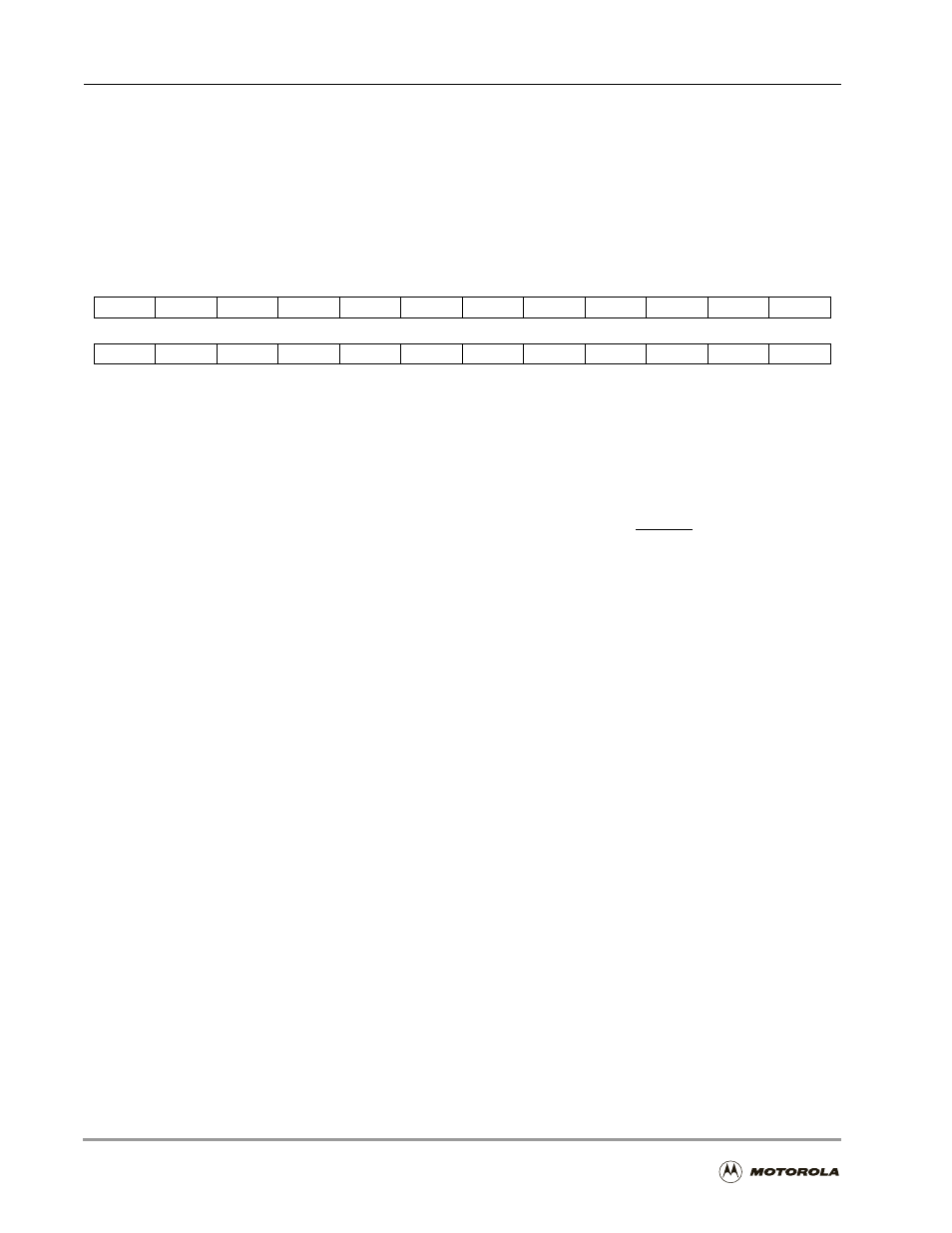
CRB is one of two read/write control registers that direct the operation of the ESSI (see
Figure 7-5). The CRB bit definitions are presented in Table 7-4. CRB controls the ESSI
multifunction signals, SC[2–0], which can be used as clock inputs or outputs, frame
synchronization signals, transmit data signals, or serial I/O flag signals.
Figure 7-5. ESSI Control Register B (CRB)
The CRB contains the serial output flag control bits and the direction control bits for the serial
control signals. Also in the CRB are interrupt enable bits for the receiver and the transmitter.
Bit settings of the CRB determines how many transmitters are enabled: 0, 1, 2, or 3. The CRB
settings also determine the ESSI operating mode. Either a hardware
RESET
signal or a
software RESET instruction clears all the bits in the CRB. Table 7-2, Mode and Signal
Definitions, on page 7-5 summarizes the relationship between the ESSI signals
SC[2–0]
,
SCK
,
and the CRB bits.
The ESSI has two serial output flag bits, OF1 and OF0. The normal sequence follows for
setting output flags when transmitting data (by transmitter 0 through the
STD
signal only).
1.
Wait for TDE (TX0 empty) to be set.
2.
Write the flags.
3.
Write the transmit data to the TX register
Bits OF0 and OF1 are double-buffered so that the flag states appear on the signals when the
TX data is transferred to the transmit shift register. The flag bit values are synchronized with
the data transfer. The timing of the optional serial output signals
SC[2–0]
is controlled by the
frame timing and is not affected by the settings of TE2, TE1, TE0, or the receive enable (RE)
bit of the CRB.
The ESSI has three transmit enable bits (TE[2–0]), one for each data transmitter. The process
of transmitting data from TX1 and TX2 is the same. TX0 differs from these two bits in that it
can also operate in Asynchronous mode. The normal transmit enable sequence is to write data
to one or more transmit data registers (or the Time Slot Register (TSR)) before you set the TE
bit. The normal transmit disable sequence is to set the Transmit Data Empty (TDE) bit and
then to clear the TE, Transmit Interrupt Enable (TIE), and Transmit Exception Interrupt
23
22
21
20
19
18
17
16
15
14
13
12
REIE
TEIE
RLIE
TLIE
RIE
TIE
RE
TE0
TE1
TE2
MOD
SYN
11
10
9
8
7
6
5
4
3
2
1
0
CKP
FSP
FSR
FSL1
FSL0
SHFD
SCKD
SCD2
SCD1
SCD0
OF1
OF0
(ESSI0 X:$FFFFB6, ESSI1 X:$FFFFA6)
