Motorola DSP56301 User Manual
Page 186

Host-Side Programming Model
6
-68
DSP56301 User’s Manual
6.8.10
Header Type/Latency Timer Configuration Register
(CHTY/CLAT/CCLS)
r (
A PCI-standard read/write register mapped into the PCI configuration space in PCI mode or
in mode 0 (DCTR[HM]
=
$1 or $0). The CHTY/CLAT/CCLS is accessed when a
configuration read/write command is in progress and the PCI address is $0C. In
Self-Configuration mode (DCTR[HM]] = $5), the DSP56300 core can indirectly access the
CLAT (see Section 6.5.5, Self-Configuration Mode (DCTR[HM] = $5), on page 6-16). The
CHTY/CLAT/CCLS is written in accordance with the byte enables. Byte lanes that are not
enabled are not written and the corresponding bits remain unchanged. The host can access
CHTY/CLAT/CCLS only when the HI32 is in PCI mode (HM
≠
$1).
31
30
29
28
27
26
25
24
23
22
21
20
19
18
17
16
HT7
HT6
HT5
HT4
HT3
HT2
HT1
HT0
15
14
13
12
11
10
9
8
7
6
5
4
3
2
1
0
LT7
LT6
LT5
LT4
LT3
LT2
LT1
LT0
CLS7 CLS6 CLS5 CLS4 CLS3 CLS2 CLS2 CLS0
Not implemented. Read and write as zero for future compatibility.
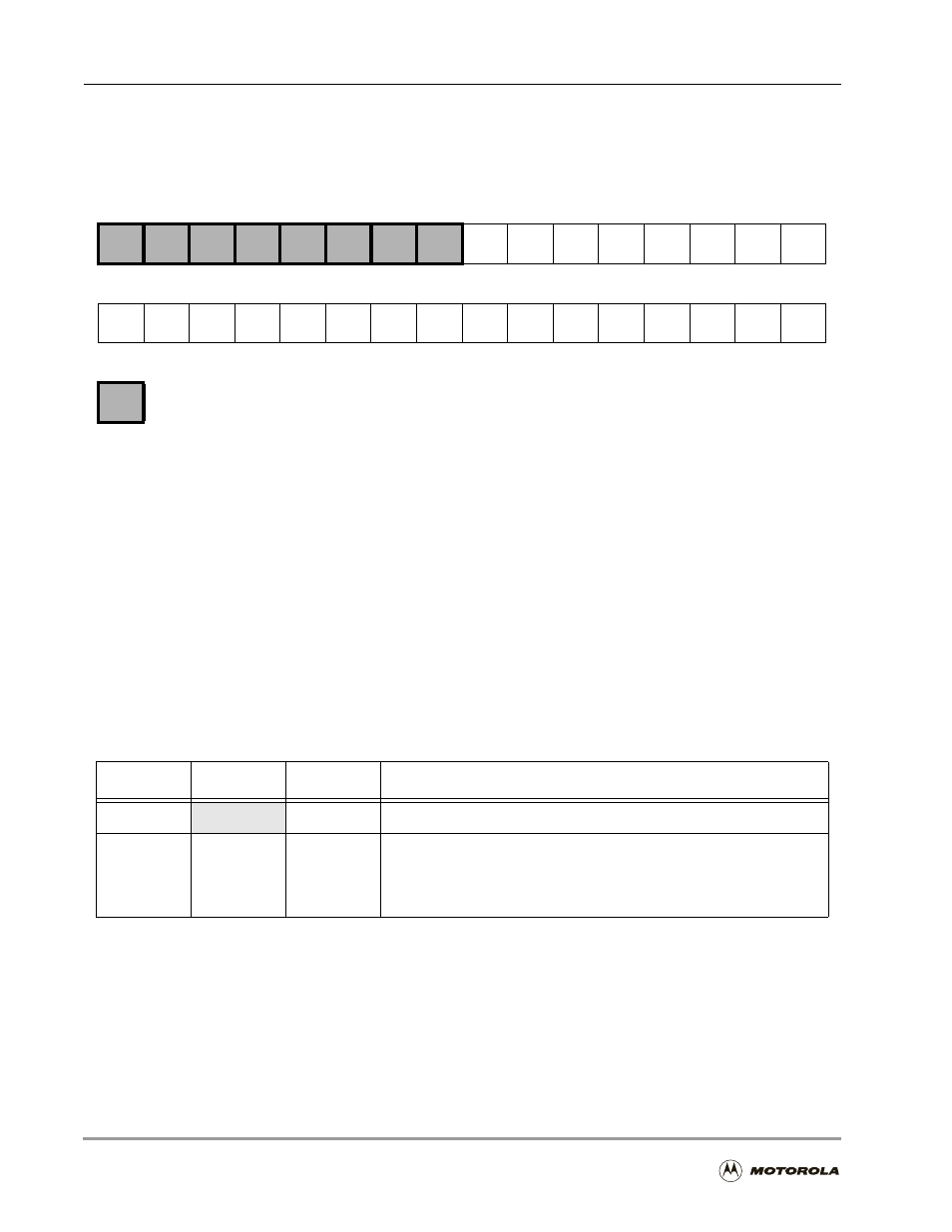
Figure 6-19. Header Type/Latency Timer Configuration Register (CHTY/CLAT/CCLS)
Table 6-28. Header Type/Latency Timer Configuration Register (CHTY/CLAT/CCLS)
Bit Definitions
Bit Number
Bit Name
Reset Value
Description
31–24
0
Not implemented. Write to zero for future compatibility.
23–16
HT[7–0]
0
Header Type (hardwired to $00)
Read-only bits that identify the layout of bytes $10-$3F in the
configuration space and also whether the device contains multiple
functions.
