Motorola DSP56301 User Manual
Page 73

Memory Maps
Memory Configuration
3
-13
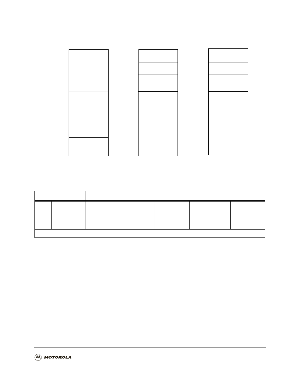
Figure 3-7. Switched Program RAM and Instruction Cache Enabled (1, 1, 0)
Program
$FFFFFF
$000000
Internal
External
X Data
$FFFFFF
$000000
$000C00
External
Internal X Data
RAM (3K)
Internal I/O
Y Data
$FF0000
$FFFF80
Bootstrap ROM
1
Internal—
Reserved
$FF00C0
External
Internal—
Reserved
$FFF000
$FF0000
$FFFFFF
$000000
External
Internal Y Data
RAM (3K)
External I/O
$FFFF80
External
Internal—
Reserved
$FFF000
$FF0000
(128 words)
(128 words)
Bit Settings
Memory Configuration
CE
MS
SC
Program RAM
X Data RAM
Y Data RAM
Cache
Addressable
Memory Size
1
1
0
1 K
$000–$3FF
3 K
$000–$BFF
3 K
$000–$BFF
1 K
not addressable
16 M
Note:
1.
Address range is for 3 K bootstrap space.
Program RAM
(1K)
$000C00
$000400
NOTE: External program memory begins immediately after the internal program memory. The
internal memory modules that are mapped to the addresses $000400–$000800 are used as
Instruction Cache space when the Instruction Cache is enabled, and these addresses become
part of the external P memory space.
