3 host command vector register (hcvr), Host command vector register (hcvr) -59, 3 host command vector register (hcvr) – Motorola DSP56301 User Manual
Page 177

Host-Side Programming Model
Host Interface (HI32)
6
-59
6.8.3
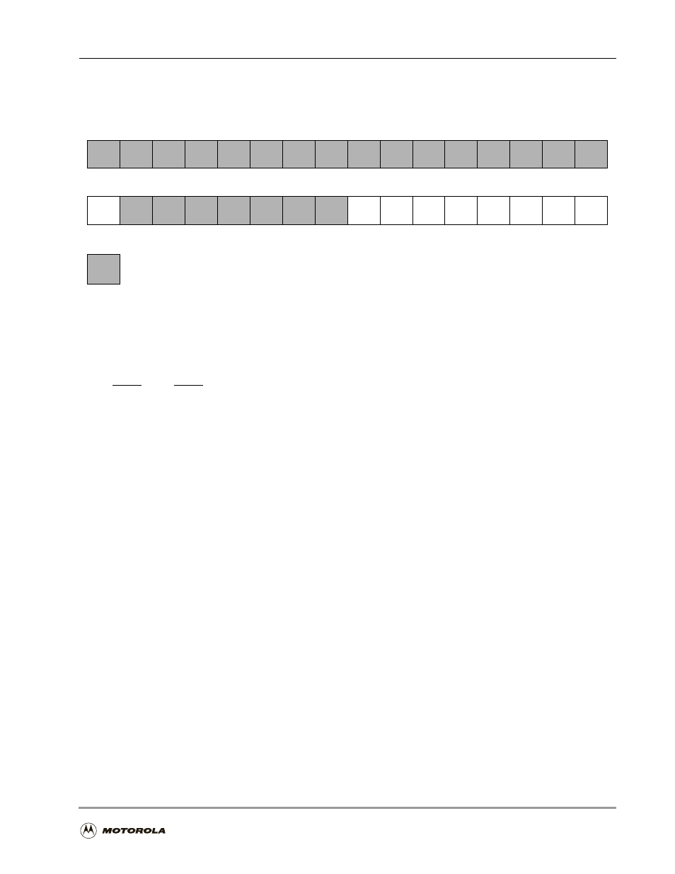
Host Command Vector Register (HCVR)
)
The HCVR is a 32-bit read/write register by which the host processor causes the DSP56300
core to execute a vectored interrupt. The host command feature is independent of any of the
data transfer mechanisms in the HI32. It can cause any of the 128 possible interrupt routines
in the DSP to be executed. The HCVR is written in accordance with the byte enables
(
HC3
/
HBE3
-
HC0
/
HBE0
pins). Byte lanes that are not enabled are not written and the
corresponding bits remain unchanged.
n
When the HCVR is read to the PCI bus (DCTR[HM]
=
$1), the
HAD[31
–
0]
pins are
driven with the HCVR data during a read access; and these pins are written to the
HCVR in a write access.
n
In a 24-bit data Universal Bus mode (DCTR[HM]
=
$2 or $3 and HCTR[HTF] = $0 or
HCTR[HRF] = $0), the
HD[23
–
0]
pins are driven with the three least significant bytes
of the HCVR in a read access;
HD[23–0]
are written to the three least significant bytes
of the HCVR, the most significant portion is zero filled during the HCVR write.
n
In a 16-bit data Universal Bus mode (DCTR[HM]
=
$2 or $3 and HCTR[HTF]
≠
$0 or
HCTR[HRF]
≠
$0), the
HD[15
–
0]
pins are driven with the two least significant bytes of
the HCVR in a read access;
HD[15
–
0]
are written to the two least significant bytes of
the HCVR, the most significant portion is zero filled during the HCVR write.
n
In PCI mode (DCTR[HM] = $1) memory space transactions, the HCVR is accessed if
the PCI address is HI32_base_address: $018.
n
In a Universal Bus mode (DCTR[HM]
=
$2 or $3), the HCVR is accessed if the
HA[10–3]
value matches the HI32 base address (see Section 6.8.11, Memory Space
Base Address Configuration Register (CBMA), on page 6-70) and the HA[2–0] value
is $6.
31
30
29
28
27
26
25
24
23
22
21
20
19
18
17
16
15
14
13
12
11
10
9
8
7
6
5
4
3
2
1
0
HNMI
HV6
HV5
HV4
HV3
HV2
HV1
HV0
HC
UBM
PCI
UBM
PCI
UBM
PCI
UBM
PCI
UBM
PCI
UBM
PCI
UBM
PCI
UBM
PCI
Reserved. Read as zero. Write to zero for future compatibility.
UBM = Universal Bus mode
PCI = PCI mode
Figure 6-15. Host Command Vector Register (HCVR)
