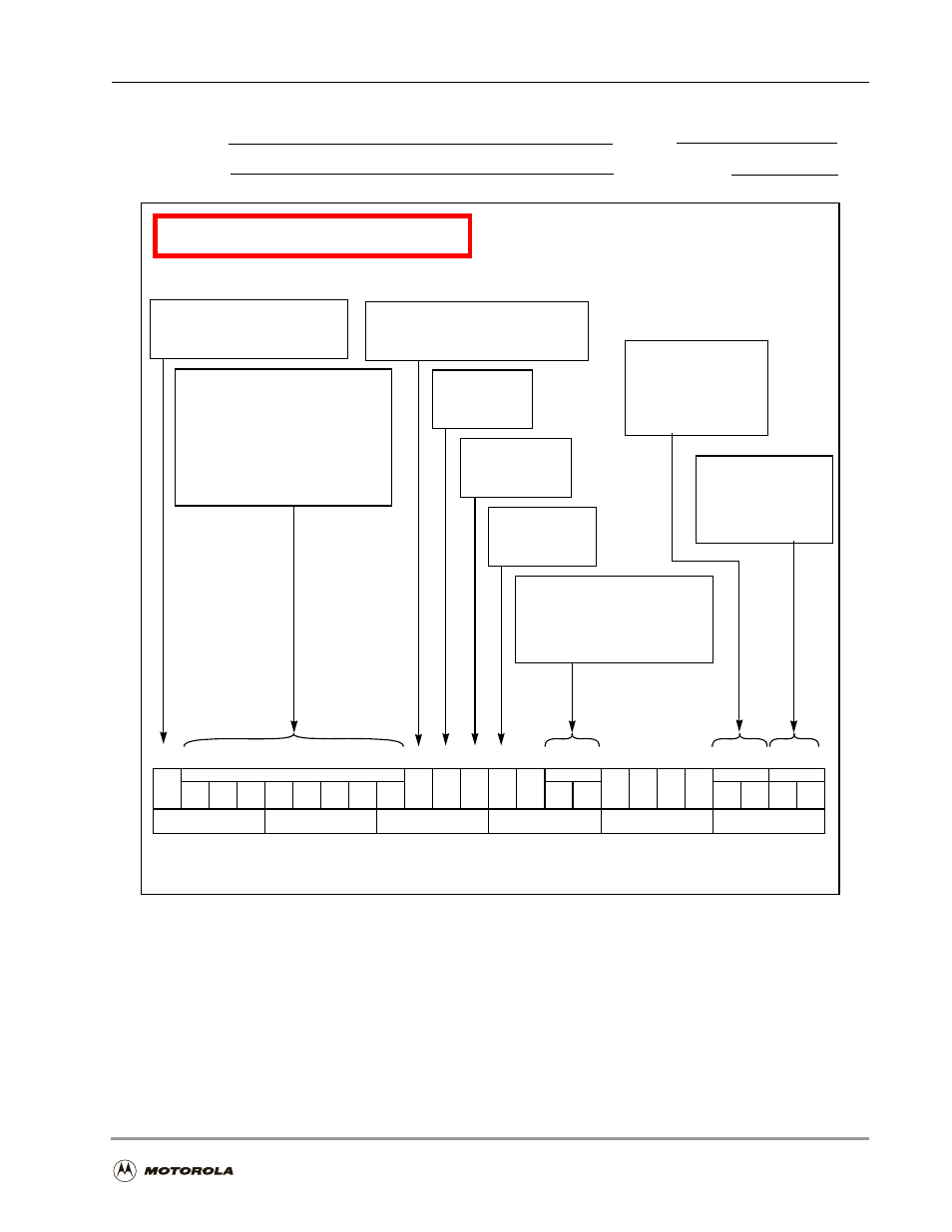
Figure b-7, Dram control register (dcr), Bus interface unit – Motorola DSP56301 User Manual
Page 331

Programming Sheets
Programming Reference
B
-19
Figure B-7. DRAM Control Register (DCR)
Bus Interface Unit
DRAM Control Register (DCR)
Reset = $000000
Refresh Request Rate, Bits 22–15
Refresh Prescaler, Bit 23
0 = Prescaler bypassed
1 = Divide-by-64 prescaler used
NOTE: All DCR bits are read/write control bits.
These read/write control bits define
the refresh request rate. The bits
specify a divide from 1–256
(BRF[7–0] = $00–$FF). A refresh
request is generated every time
the refresh counter reaches zero,
Application:
Date:
Programmer:
Sheet 2 of 3
15 14 13 12 11 10
9
8
7
6
5
4
3
2
1
0
19 18 17 16
23 22 21 20
BRP
BRF[7–0]
BPS[1–0]
BCW[1–0]
X:$FFFFFA Read/Write
BRW[1–0]
BSTR BREN BME BPLE
if the refresh counter is enabled
(i.e., BREN = 1).
Bus Software Triggered
0 = Refresh complete/reset
1 = Software triggered refresh request
Bus Refresh
0 = Disable
1 = Enable
Bus Mastership
0 = Disable
1 = Enable
Bus Page Logic
0 = Disable
1 = Enable
*
= Reserved, Program as 0
*
0
*
0
*
0
*
0
*
0
Bus DRAM Page Size, Bits 9–8
00 = 9-bit column width, 512
01 = 10-bit column width, 1 K
10 = 11-bit column width, 2 K
11 = 12-bit column width, 4 K
Bus Row Out-of-Page
00 = 4 wait states
01 = 8 wait states
10 = 11 wait states
11 = 15 wait states
Bus In-Page
00 = 1 wait state
01 = 2 wait states
10 = 3 wait states
11 = 4 wait states
Refresh, Bit 14
Enable, Bit 13
Enable, Bit 12
Enable, Bit 11
Wait States, Bits 1–0
Wait States, Bits 3–2
