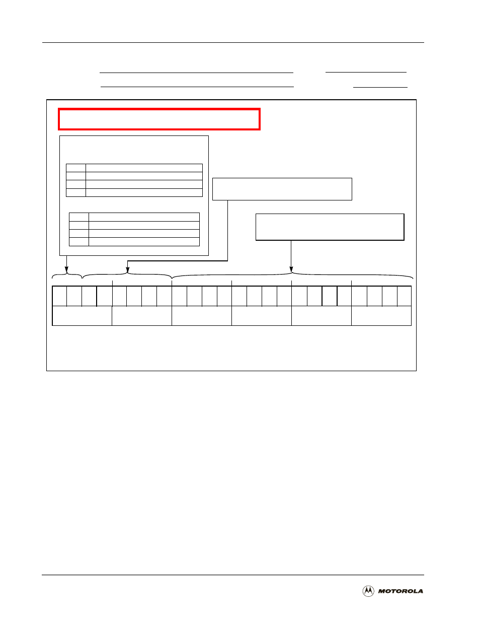
B-12, Figure b-12, Dsp pci master control register (dpmc) – Motorola DSP56301 User Manual
Page 336: Host processor (hi32), Or the system is in self-configuration mode

Programming Sheets
B
-24
DSP56301 User’s Manual
Figure B-12. DSP PCI Master Control Register (DPMC)
Host Processor (HI32)
DSP PCI Master Control Register (DPMC)
Reset = $000000
15 14 13 12 11 10
9
8
7
6
5
4
3
2
1
0
AR21
AR18
AR17
19 18 17 16
23 22 21 20
AR30
BL3
BL2
BL4
BL5
AR20
BL0
AR31
AR28
AR25
AR23
Note: All bits work only in PCI mode (DCTR[HM] = $1). You can write to the DPMC only if MARQ is set
Address: X:FFFFC7 Read/Write
Application:
Date:
Programmer:
Sheet 3 of 10
FC1
FC0
BL1
AR29
AR27
AR26
AR24
AR22
AR19
AR16
or the system is in Self-Configuration mode.
Data Transfer Format Control
, Bits 23–22
00
32-bit data mode
01
Data to HAD[31–0] right-aligned and zero extended in MSB
10
Data to HAD[31–0] right-aligned and sign extended in MSB
11
Data to HAD[31–0] left-aligned and zero filled in LSB
HI32-PCI data transfer formats, as follows:
PCI Data Burst Length, Bits 21–16
The value is the desired number of burst
DSP PCI Transaction Address (High), Bits 15–0
The two most significant bytes of the 32-bit
accesses – 1.
00
32-bit data mode
01
3 LSB PCI data to DRXR from HAD[23–0]
10
3 LSB PCI data to DRXR from HAD[23–0]
11
3 MSB PCI data to DRXR from HAD[31–8]
PCI Host-to-DSP
PCI DSP-to-Host (data in DTXM)
Note: LSB = least significant byte; MSB = most significant byte
PCI transaction address.
