6 bus interface unit (biu) registers, 1 bus control register, Bus interface unit (biu) registers -22 – Motorola DSP56301 User Manual
Page 96: Bus control register -22, Bus control register (bcr) -22, Bus control register (bcr) bit definitions -22, 6 bus interface unit (biu) registers, 1 bus control register, Bus control register (bcr), Dram control register (dcr)

Bus Interface Unit (BIU) Registers
4
-22
DSP56301 User’s Manual
4.6
Bus Interface Unit (BIU) Registers
The three Bus Interface Unit (BIU) registers configure the external memory expansion port
(Port A). They include the following:
n
Bus Control Register (BCR)
n
DRAM Control Register (DCR)
n
Address Attribute Registers (AAR[3–0])
To use Port A correctly, configure these registers as part of the bootstrap process. The
following subsections describe these registers.
4.6.1
Bus Control Register
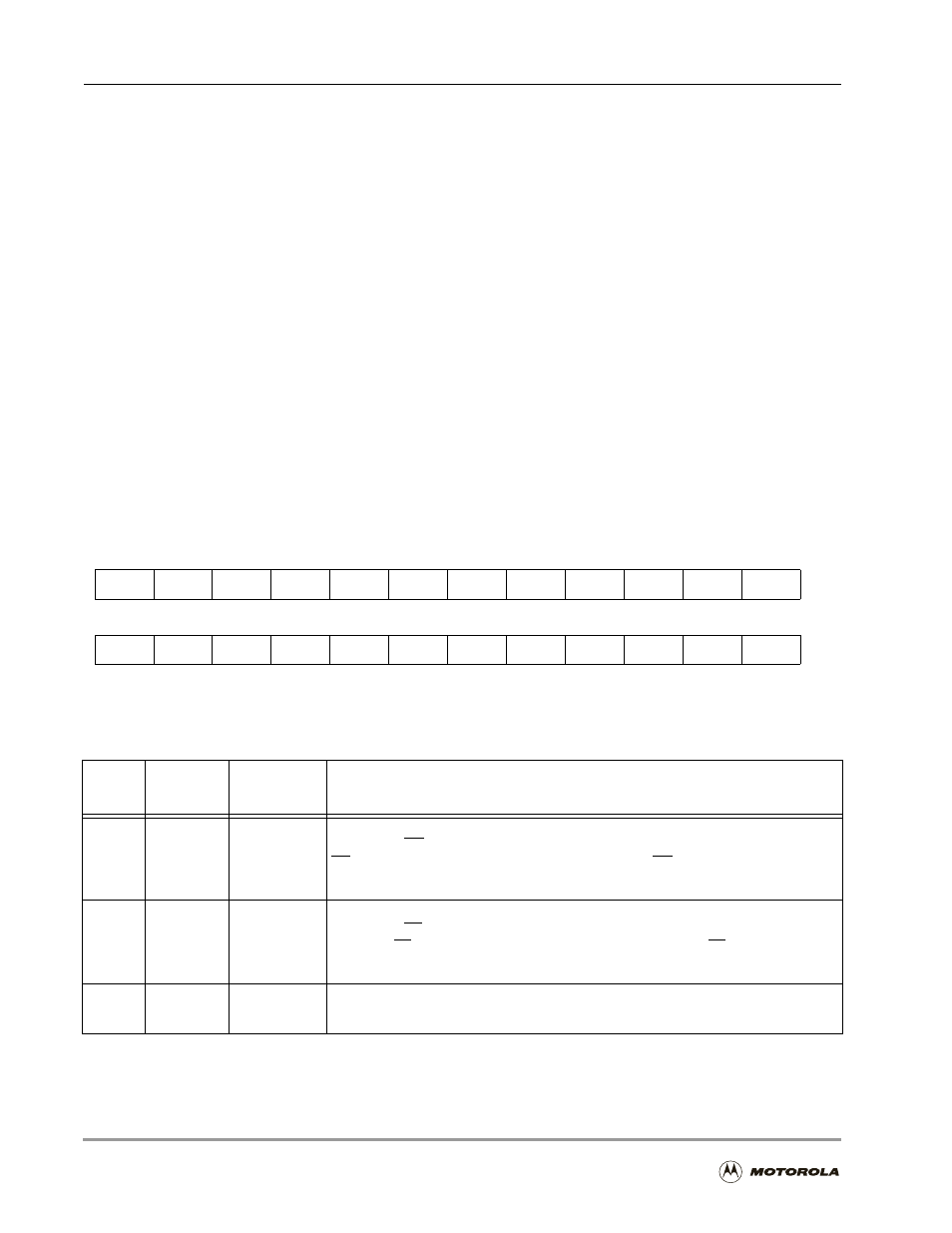
The Bus Control Register (BCR), depicted in Figure 4-6, is a read/write register that controls
the external bus activity and Bus Interface Unit (BIU) operation. All BCR bits except bit 21,
BBS, are read/write bits. The BCR bits are defined in Table 4-9.
Figure 4-6. Bus Control Register (BCR)
Table 4-9. Bus Control Register (BCR) Bit Definitions
Bit
Number
Bit Name
Reset Value
Description
23 BRH
0
Bus Request Hold
Asserts the BR signal, even if no external access is needed. When BRH is set, the
BR signal is always asserted. If BRH is cleared, the BR is asserted only if an
external access is attempted or pending.
22
BLH
0
Bus Lock Hold
Asserts the BL signal, even if no read-modify-write access is occurring. When BLH
is set, the BL signal is always asserted. If BLH is cleared, the BL signal is asserted
only if a read-modify-write external access is attempted.
21
BBS
0
Bus State
This read-only bit is set when the DSP is the bus master and is cleared otherwise.
23
22
21
20
19
18
17
16
15
14
13
12
BRH
BLH
BBS
BDFW4 BDFW3 BDFW2 BDFW1 BDFW0 BA3W2 BA3W1 BA3W0 BA2W2
11
10
9
8
7
6
5
4
3
2
1
0
BA2W1 BA2W0 BA1W4 BA1W3 BA1W2 BA1W1 BA1W0 BA0W4 BA0W3 BA0W2 BA0W1 BA0W0
