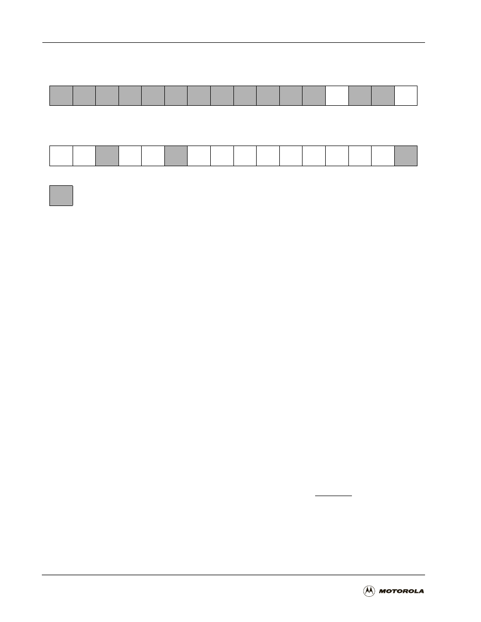
1 hi32 control register (hctr), Hi32 control register (hctr) -48, Host interface control register (hctr) -48 – Motorola DSP56301 User Manual
Page 166: 1 hi32 control register (hctr)

Host-Side Programming Model
6
-48
DSP56301 User’s Manual
6.8.1
HI32 Control Register (HCTR)
The HCTR is a 32-bit read/write control register by which the host processor controls the
HI32 interrupts, flags, semaphores, data transfer formats, and operation modes. The HCTR
bits affect the HI32 logic upon the completion of the transaction in which they were written.
n
In PCI mode (DCTR[HM]
=
$1), the
HAD[31– 0]
pins are driven with HCTR data
during a read access; and the pins are written to the HCTR in a write access. In PCI
mode memory space transactions, the HCTR is accessed if the PCI address is
HI32_base_address: $010.
n
In a 24-bit data Universal Bus mode (DCTR[HM]
=
$2 or $3 and HCTR[HTF] = $0 or
HCTR[HRF] = $0), the
HD[23–0]
pins are driven with the three least significant HCTR
bytes during a read access;
HD[23–0]
are written to the three least significant HCTR
bytes in a write access.
n
In a 16-bit data Universal Bus mode (DCTR[HM]
=
$2 or $3 and HCTR[HTF]
≠
$0 or
HCTR[HRF]
≠
$0), the
HD[15–0]
pins are driven with the two least significant bytes of
the HCTR in a read access;
HD[15–0]
are written to the two least significant bytes of the
HCTR, the most significant portion is zero filled during the HCTR write.
n
In a Universal Bus mode (DCTR[HM]
=
$2 or $3), the HCTR is accessed if the
HA[10–3] value matches the HI32 base address (see Section 6.8.11, Memory Space
Base Address Configuration Register (CBMA), on page 6-70) and the HA[2–0] value
is $4.
The HCTR is written in accordance with the byte enables (
HC[3–0]/HBE[3–0]
pins). Byte lanes
that are not enabled are not written, and the corresponding bits remain unchanged.
31
30
29
28
27
26
25
24
23
22
21
20
19
18
17
16
TWSD
HS2
PCI
UBM
PCI
15
14
13
12
11
10
9
8
7
6
5
4
3
2
1
0
HS1
HS0
HRF1 HRF0
HTF1 HTF0
SFT DMAE HF2
HF1
HF0 RREQ TREQ
UBM
PCI
UBM
PCI
UBM
PCI
UBM
PCI
UBM
PCI
UBM
PCI
UBM
PCI
UBM
UBM
PCI
UBM
PCI
UBM
PCI
UBM
PCI
UBM
PCI
Reserved. Read as zero. Write to zero for future compatibility.
UB = Universal Bus mode
PCI = PCI mode
Figure 6-13. Host Interface Control Register (HCTR)
