2 list of cn1 terminals, Cn1 terminal layout – Yaskawa Large Capacity Sigma II Series User Manual
Page 50
2.4 I/O Signals
2-23
2
2.4.2 List of CN1 Terminals
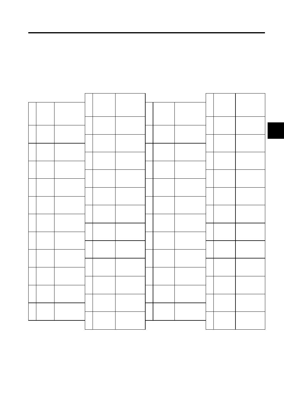
The following diagram shows the layout and specifications of CN1 terminals.
CN1 Terminal Layout
Note: 1. Do not use unused terminals for relays.
2. Connect the shield of the I/O signal cable to the connector shell. Connect to the FG (frame
ground) at the SERVOPACK-end connector.
1
SG
GND
26 /V-CMP-
(/COIN-)
Speed
Coincidence
Detection Out-
put
2
SG
GND
27 /TGON+
TGON signal
output
3
PL1
Open-collec-
tor reference
power supply
28 /TGON-
TGON signal
output
4
SEN
SEN signal
input
29 /S-RDY+ Servo ready
output
5
V-REF
Speed Refer-
ence Input
30 /S-RDY-
Servo ready
output
6
SG
GND
31 ALM+
Servo alarm
output
7
PULS
Reference
pulse input
32 ALM-
Servo alarm
output
8
/PULS
Reference
pulse input
33 PAO
PG divided out-
put phase A
9
T-REF
Torque Refer-
ence Input
34 /PAO
PG divided
output phase
A
10 SG
GND
35 PBO
PG divided out-
put phase B
11 SIGN
Reference sign
input
36 /PBO
PG divided
output phase B
12 /SIGN
Reference sign
input
37 ALO1
Alarm code
outputs
13 PL2
Open-collec-
tor reference
power supply
38 ALO2
Alarm code
outputs
14 /CLR
Clear input
39 ALO3
(open-collector
output)
15 CLR
Clear input
40 /S-ON
Servo ON
input
16
−
−
41 P-CON
P operation
input
17
−
−
42 P-OT
Forward over-
travel input
18 PL3
Open-collec-
tor reference
power supply
43 N-OT
Reverse over-
travel input
19 PCO
PG divided
output phase C
44 /ALM-
RST
Alarm reset
input
20 /PCO
PG divided
output phase C
45 /P-CL
Forward cur-
rent limit ON
input
21 BAT (+)
Battery (+)
46 /N-CL
Reverse cur-
rent limit ON
input
22 BAT (-) Battery (-)
47 +24V
-IN
External input
power supply
23
−
−
48 PSO
Phase-S sig-
nal output
24
−
−
49 /PSO
Phase-S signal
output
25 /V-CMP+
(/COIN+)
Speed coinci-
dence detec-
tion output
50
−
−