Appendix c timing diagrams in flash memory mode – FUJITSU F2MCTM-16LX User Manual
Page 652
636
APPENDIX
APPENDIX C
Timing Diagrams in Flash Memory Mode
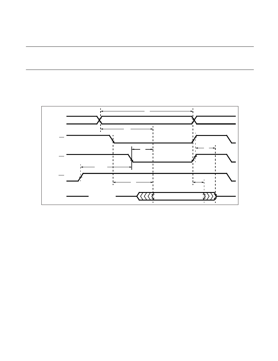
Each timing diagram for the external pins of the Flash devices in MB90360 series during
Flash Memory mode is shown below.
■
Data Read by Read Access
Figure C-1 Timing Diagram for Read Access
AQ16
to
AQ0
CE
OE
WE
DQ7
to
DQ0
t
RC
t
ACC
t
OE
t
OEH
t
CE
t
DF
t
OH
High-Z
Address stable
Output defined
See also other documents in the category FUJITSU Hardware:
- XG Series P3NK-4452-01ENZD (614 pages)
- FPCAC14C (1 page)
- MCJ3230SS (161 pages)
- MBA3073NC (138 pages)
- T5140 (102 pages)
- T5140 (76 pages)
- MAM3367MC/MP (152 pages)
- MPC3045AH (185 pages)
- MB2142-02 (23 pages)
- MB15F86UL (6 pages)
- MHS2030AT (40 pages)
- MHW2100BS (296 pages)
- MHK2060AT (227 pages)
- Disk Drives MHK2060AT (227 pages)
- MCM3064SS (170 pages)
- Mainboard D1561 (45 pages)
- MHC2040AT (219 pages)
- D1961 (45 pages)
- DISK DRIVES MHM2100AT (231 pages)
- MHR2010AT (250 pages)
- MHZ2120BJ (320 pages)
- MCE3064AP (175 pages)
- LQFP-64P (16 pages)
- Solaris PCI GigabitEthernet 3.0 (115 pages)
- MAY2036RC (94 pages)
- MAB3091 (142 pages)
- MPE3XXXAT (191 pages)
- MHV2040AH (40 pages)
- MHW2040AC (278 pages)
- ETERNUSmgr P2X0-0202-01EN (64 pages)
- VSS Hardware Provider 2.1 (134 pages)
- MAG3182FC (61 pages)
- MAU3147NC/NP (130 pages)
- MAX3147RC (94 pages)
- MHV2160BT (296 pages)
- MHV2040AT (280 pages)
- MAW3300NC/NP (130 pages)
- DeskPower E623 (50 pages)
- MAG3182LC (133 pages)
- OPTICAL DISK DRIVES MDG3064UB (42 pages)
- MHF2021AT (225 pages)
- MHR2040AT (40 pages)
- Single Drive FTM7926FB (1 page)
- PG-FCS103 (98 pages)
- MAS3735FC (114 pages)