FUJITSU F2MCTM-16LX User Manual
Page 145
129
CHAPTER 7 RESETS
■
Correspondence between reset cause bits and reset causes
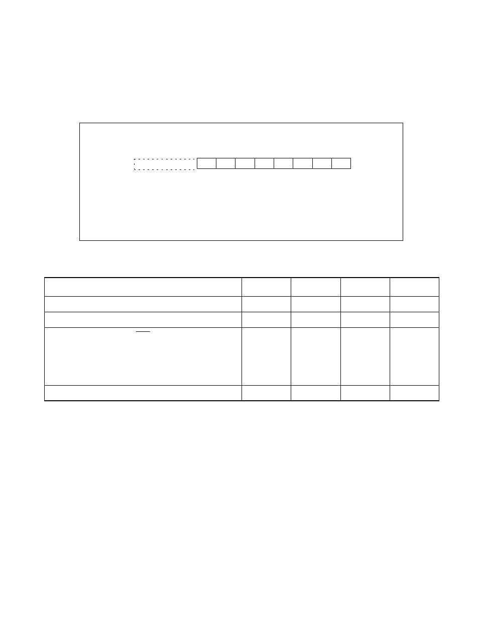
Figure 7.5-2 shows the configuration of the reset cause bits of the watchdog timer control register (WDTC).
Table 7.5-1 maps the correspondence between the reset cause bits and reset causes. See “Watchdog timer
control register (WDTC)” in "12.1 Overview of Watchdog Timer", for details.
Figure 7.5-2 Configuration of Reset Cause Bits (watchdog timer control register)
Watchdog timer control register (WDTC)
Address
bit15
........ bit8
bit7
bit6
bit5
bit4
bit3
bit2
bit1
bit0
Initial value
0000A8
H
(TBTC)
PONR
−
WRST ERST SRST
WTE
WT1
WT0
XXXXX111
B
R
−
R
R
R
W
W
W
R
: Read only
W
: Write only
X
: Undefined
Table 7.5-1 Correspondence between Reset Cause Bits and Reset Causes
Reset cause
PONR
WRST
ERST
SRST
Generation of power-on reset request
1
X
X
X
Generation of reset request due to watchdog timer overflow
∆
1
∆
∆
External reset request from RST pin,
Low voltage detection reset (product with T-suffix)
*1
CPU operation detection reset (product with T-suffix)
*2
Clock supervisor reset
(MB90F367/T(S), MB90367/T(S))
∆
∆
1
∆
Generation of software reset request
∆
∆
∆
1
∆: Previous state retained
X: Undefined
*1: When the low voltage detection reset request is used, the CPUF bit of the low voltage/CPU operation detection reset
control register (LVRC) is also set to "1".
*2: When the CPU operation detection reset request is used, the CPUF bit of the low voltage/CPU operation detection reset
control register (LVRC) is also set to "1".