3 ppgc/d count clock select register (ppgcd), Ppgc/d count clock select register (ppgcd) – FUJITSU F2MCTM-16LX User Manual
Page 312
296
CHAPTER 16 8-/16-BIT PPG TIMER
16.3.3
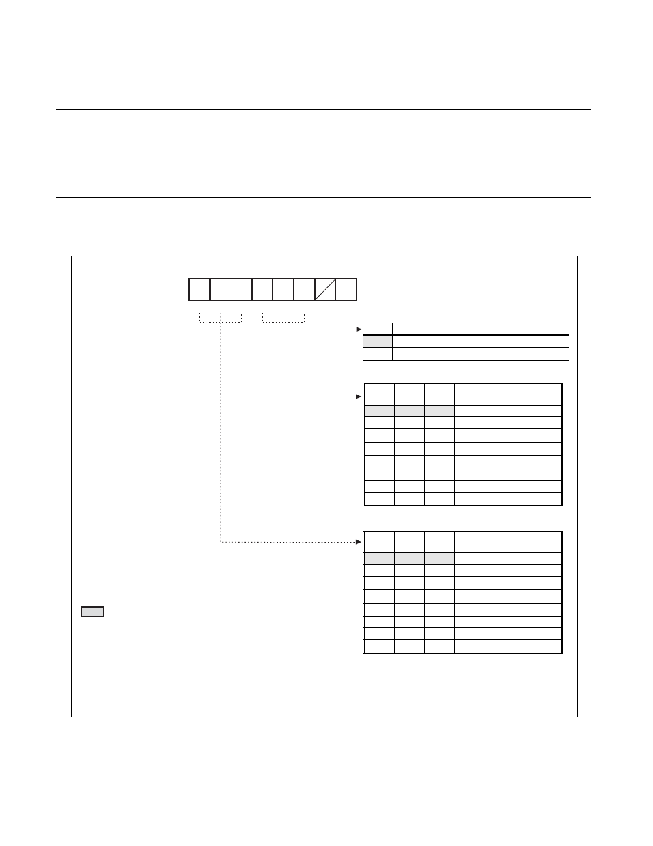
PPGC/D Count Clock Select Register (PPGCD)
The PPGC/D count clock select register selects the count clock of the 8-/16-bit PPG
timers C and D and the output pin.
This section explains the PPGCD function only. The PPGEF has the same function as
the PPGCD, and the 8-/16-bit PPG timers E and F are set.
■
PPGC/D Count Clock Select Register (PPGCD)
Figure 16.3-4 PPGC/D Count Clock Select Register (PPGCD)
4
5
3
2
1
0
7
6
−
R/W
R/W
R/W
R/W
R/W
R/W
HCLK
φ
R/W
X
−
0
0
0
0
0
0
X
0
B
R/W
PCS2 PCS1 PCS0 PCM2 PCM1 PCM0
REV
Address:
chD
PPGCD
00004A
H
Other channel:
chF
PPGEF
00004E
H
: Read/Write
: Indeterminate
: Undefined
: Reset value
: Oscillation clock
: Machine clock frequency
bit 0
REV
PPG output pin select bit
0
Output pulse from standard output pin
1
Switch output pin between PPGn and PPGm
Reset value
bit 7
bit 6
bit 5
PCS2
PCS1
PCS0
PPGD
count clock select bits
0
0
0
1/
φ
(41.7 ns)
0
0
1
2/
φ
(83.3 ns)
0
1
0
2
2
/
φ
(167 ns)
0
1
1
2
3
/
φ
(333 ns)
1
0
0
2
4
/
φ
(667 ns)
1
0
1
Setting disable
1
1
0
Setting disable
1
1
1
2
9
/HCLK(128
µ
s)
bit 4
bit 3
bit 2
PCM2 PCM1 PCM0
PPGC
count clock select bits
0
0
0
1/
φ
(41.7 ns)
0
0
1
2/
φ
(83.3 ns)
0
1
0
2
2
/
φ
(167 ns)
0
1
1
2
3
/
φ
(333 ns)
1
0
0
2
4
/
φ
(667 ns)
1
0
1
Setting disable
1
1
0
Setting disable
1
1
1
2
9
/HCLK(128
µ
s)
The parenthesized values are provided when the oscillation clock operates at
4 MHz and the machine clock operates at 24 MHz.
n = C, E
m = n+1