FUJITSU F2MCTM-16LX User Manual
Page 614
598
APPENDIX
RMW
Indicates whether the instruction is a Read Modify Write instruction (reading data
from memory by the I instruction and writing the result to memory).
*: Read Modify Write instruction
-: Not Read Modify Write instruction
Note:
Cannot be used for an address that has different meanings between read and write
operations.
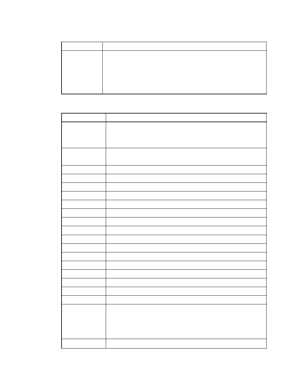
Table B.7-2 Explanation on Symbols in the Instruction List (1/2)
Symbol
Explanation
A
The bit length used varies depending on the 32-bit accumulator instruction.
Byte: Low-order 8 bits of byte AL
Word: 16 bits of word AL
Long word: 32 bits of AL and AH
AH
16 high-order bits of A
AL
16 low-order bits of A
SP
Stack pointer (USP or SSP)
PC
Program counter
PCB
Program bank register
DTB
Data bank register
ADB
Additional data bank register
SSB
System stack bank register
USB
User stack bank register
SPB
Current stack bank register (SSB or USB)
DPR
Direct page register
brg1
DTB, ADB, SSB, USB, DPR, PCB, SPB
brg2
DTB, ADB, SSB, USB, DPR, SPB
Ri
R0, R1, R2, R3, R4, R5, R6, R7
RWi
RW0, RW1, RW2, RW3, RW4, RW5, RW6, RW7
RWj
RW0, RW1, RW2, RW3
RLi
RL0, RL1, RL2, RL3
dir
Abbreviated direct addressing
addr16
Direct addressing
addr24
Physical direct addressing
ad24 0-15
Bits 0 to 15 of addr24
ad24 16-23
Bits 16 to 23 of addr24
io
I/O area (000000
H
to 0000FF
H
)
Table B.7-1 Description of Items in the Instruction List (2/2)
Item
Description