3 lin-uart pins, Lin-uart pins, Block diagram of lin-uart pins – FUJITSU F2MCTM-16LX User Manual
Page 407
391
CHAPTER 20 LIN-UART
20.3
LIN-UART Pins
This section describes the LIN-UART pins and provides a pin block diagram.
■
LIN-UART Pins
The LIN-UART pins also serve as general ports. Table 20.3-1 lists the pin functions, I/O formats, and
settings required to use LIN-UART.
See "3. DC Characteristics in ELECTRICAL CHARACTERISTICS" in the data sheet for the standard
value.
■
Block Diagram of LIN-UART Pins
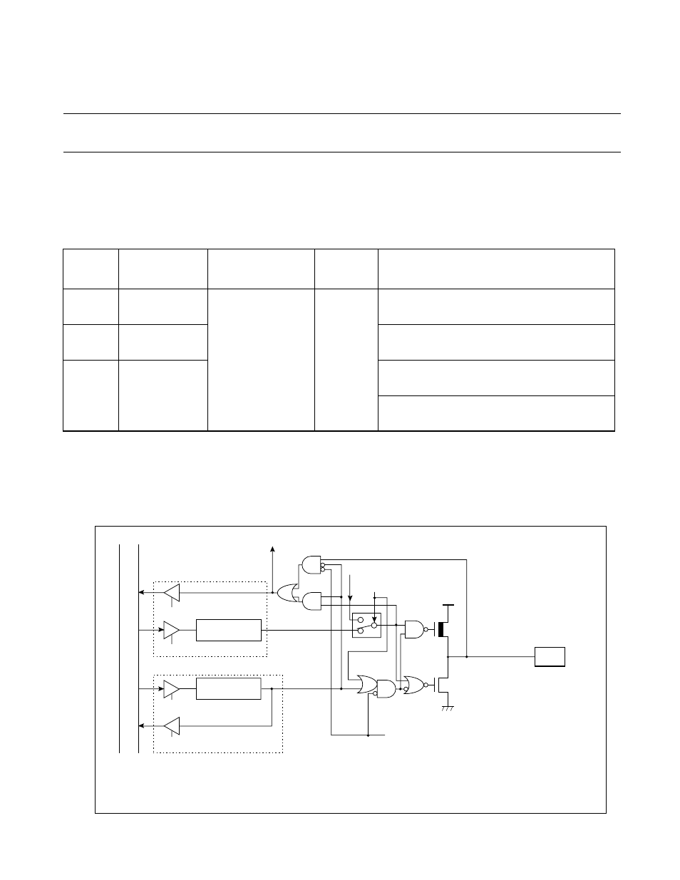
Figure 20.3-1 Block Diagram of LIN-UART Pins
Table 20.3-1 LIN-UART Pin
Pin Name
Pin Function
I/O Format
Standby
Control
Setting Required to Use Pin
P82/SIN0
P85/SIN1
Port I/O or serial
data input
CMOS output/CMOS,
Automotive input
Provided
Set as input port
(DDR: corresponding bit = 0)
P83/SOT0
P86/SOT1
Port I/O or serial
data output
Set to output enable mode
(SMRn: SOE = 1)
P84/SCK0
P87/SCK1
Port I/O or serial
clock input/output
Set as an input port when a clock is inputted
(DDR: corresponding bit = 0)
Set to output enable mode when a clock is outputted
(SMRn: SCKE = 1)
Pch
Nch
Pin
Port data register (PDR)
Resource input*
Resource output*
Resource output enable
General-purpose I/O pin/SIN
General-purpose I/O pin/SCK
General-purpose I/O pin/SOT
Standby control (SPL = 1)
Standby control: Stop mode (SPL=1), watch mode (SPL=1), timebase timer mode (SPL=1)
*: Resource I/O signals are inputted or outputted from pins having peripheral functions.
DDR read
DDR write
Direction latch
PDR read
Port direction register (DDR)
Output write
PDR read
In
ter
n
al da
ta
b
u
s