FUJITSU F2MCTM-16LX User Manual
Page 31
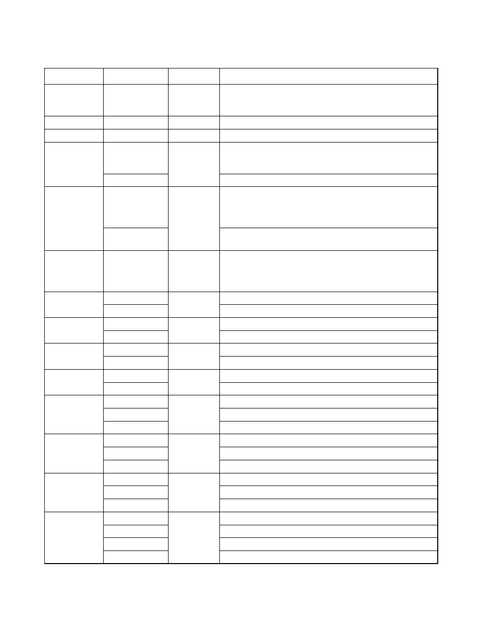
15
CHAPTER 1 OVERVIEW
26
C
I
Capacity pin for stabilizing power supply.
It should be connected to higher than or equal to 0.1
µF ceramic
capacitor.
27
X0
A
Oscillation input pin
28
X1
A
Oscillation output pin
29 to 32
P24 to P27
G
General-purpose I/O port
The register can be set to select whether to use pull-up register.
This function is enabled in single-chip mode.
IN0 to IN3
Event input pin for input capture 0 to 3.
33, 34
P22 to P23
J
General-purpose I/O port
The pull-up resistor ON/OFF can be set by setting the register.
This function becomes valid at shingle-chip mode.
High current output port
PPGF(E),
PPGD(C)
Output pin for PPG
35, 36
P20, P21
J
General-purpose I/O port
The pull-up resistor ON/OFF can be set by setting the register.
This function becomes valid at shingle-chip mode.
High current output port
37
P85
K
General-purpose I/O port
SIN1
Serial data input pin for UART1
38
P87
F
General-purpose I/O port
SCK1
Clock I/O pin for UART1
39
P86
F
General-purpose I/O port
SOT1
Serial data output pin for UART1
40
P43
F
General-purpose I/O port
TX1
TX output pin for CAN1 interface
41
P42
F
General-purpose I/O port
RX1
RX input pin for CAN1 interface
INT9R
External interrupt request input pin for INT9R (sub)
42
P83
F
General-purpose I/O port
SOT0
Serial data output pin for UART0
TOT2
Output pin for reload timer 2
43
P84
F
General-purpose I/O port
SCK0
Clock I/O pin for UART0
INT15R
External interrupt request input pin for INT15R
44
P82
K
General-purpose I/O port
SIN0
Serial data input pin for UART0
INT14R
External interrupt request input pin for INT14R
TIN2
Event input pin for reload timer 2
Table 1.5-1 Pin Description (2/3)
Pin number
Pin name
Circuit type
Functional description