3 pull-up control register (pucr), Pull-up control register (pucr), Block diagram of pull-up control register (pucr) – FUJITSU F2MCTM-16LX User Manual
Page 190
174
CHAPTER 10 I/O PORTS
10.2.3
Pull-up Control Register (PUCR)
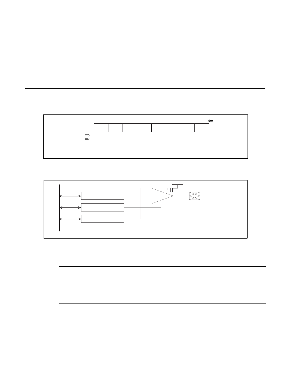
Each pin of port2 has programmable pull-up resistor. Each bit of this register controls
corresponding pull-up resistor whether to be used or not.
Figure 10.2-4 shows the pull-up control register (PUCR), and Figure 10.2-5 is the block
diagram.
■
Pull-up Control Register (PUCR)
Figure 10.2-4 Pull-up Control Register (PUCR)
■
Block Diagram of Pull-up Control Register (PUCR)
Figure 10.2-5 Block Diagram of Pull-up Control Register (PUCR)
In input mode, the pull-up resistor is controlled.
0: No pull-up resistor in input mode
1: Pull-up resistor in input mode
Note:
In output mode, this register has no meaning (no pull-up resistor).
The port direction register (DDR) determines the input-output mode.
In stop mode (SPL=1), the state with no pull-up resistor is entered (high impedance).
PU27 PU26 PU25 PU24 PU23 PU22 PU21 PU20
7
6
5
4
3
2
1
0
(R/W) (R/W) (R/W) (R/W) (R/W) (R/W) (R/W)
(0)
(0)
(0)
(0)
(0)
(0)
(0)
(0)
(R/W)
PUCR2
Bit No.
Read/Write
Initial value
Address: 00001E
H
R/W: Read/Write
Pull-up resistor (approx. 50 k
Ω
)
Port I/O
Internal data bus
Port data register
Port direction register
Pull-up control register