1 watchdog timer control register (wdtc), Watchdog timer control register (wdtc) – FUJITSU F2MCTM-16LX User Manual
Page 218
202
CHAPTER 12 WATCHDOG TIMER
12.3.1
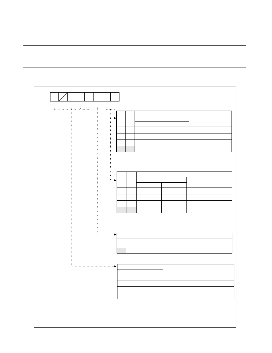
Watchdog timer control register (WDTC)
The watchdog timer control register starts and clears the watchdog timer, sets the
interval time, and holds reset factors.
■
Watchdog Timer Control Register (WDTC)
Figure 12.3-2 Watchdog Timer Control Register (WDTC)
4
5
3
2
1
6
R
R
R
R
W
W
W
0
7
XXXXX111
B
PONR
WRST ERST SRST WTE
WT1
WT0
HCLK: Oscillation clock
The parenthesized values are interval time when the oscillation clock
operates at HCLK 4 MHz.
bit1
bit0
WT1 WT0
Interval time select bit (timebase timer output select)
Interval time
Clock cycle
Min
Max
0
0
approx. 3.58 ms
approx. 4.61 ms
2
14
±
2
11
/HCLK
0
1
approx. 14.33 ms
approx. 18.3 ms
2
16
±
2
13
/HCLK
1
0
approx. 57.23 ms
approx. 73.73 ms
2
18
±
2
15
/HCLK
1
1
approx. 458.75 ms approx. 589.82 ms
2
21
±
2
18
/HCLK
Reset value
bit2
WTE
Watchdog timer control bit
0
First programming after reset:
Start up the watchdog timer
Twice or more programming after reset :
Clear the watchdog timer
1
No effect
SCLK: Sub clock*
2
The parenthesized values are interval time when the oscillation clock
bit1
bit0
WT1 WT0
Interval time select bit (watch timer output select)
Interval time
Clock cycle
Min
Max
0
0
approx. 0.457 s
approx. 0.576 s
2
12
±
2
9
/SCLK
0
1
approx. 3.584 s
approx. 4.608 s
2
15
±
2
12
/SCLK
1
0
approx. 7.168 s
approx. 9.216 s
2
16
±
2
13
/SCLK
1
1
approx. 14.336 s approx. 18.432 s
2
17
±
2
14
/SCLK
bit7
bit5
bit4
bit3
Reset factor bit
Reset factor
PONR WRST ERST SRST
1
X
X
X
Power-on reset
*
1
1
*
1
*
1
Watchdog reset
*
1
*
1
1
*
1
External reset (Low level input to RST pin)
*
1
*
1
*
1
1
Software reset (write "1" to RST bit)
R : Read only
W : Write only
X : Undefined
*1 : The previous state is held.
*2 : However, SCLK is 2 division or 4 division of the clock inputted to the low-speed oscillation pin (X0A and
X1A) or internal CR oscillation clock. The division ratio is set by the SCDS bit of the PLL/subclock control
register (PSCCR). (See "CHAPTER 5 CLOCKS".)
See Table 12.1-1 for the interval time.
Address
0000A8
H