1 i/o ports, I/o ports – FUJITSU F2MCTM-16LX User Manual
Page 184

168
CHAPTER 10 I/O PORTS
10.1
I/O Ports
Each pin of the ports can be specified as input or output using the port direction
register (DDR) if the corresponding peripheral does not use the pin. When a pin is
specified as input, the logic level at the pin is read. When a pin is specified as output,
the port data register value is read. The above also applies to a read operation for the
read-modify-write instructions.
■
I/O Ports
When a pin is used as an output of other peripheral function, the logic level at the pin is read regardless of
the port data register value.
It is generally recommended that the read-modify-write instructions should not be used for setting the port
data register prior to setting the port as an output. This is because the read-modify-write instruction in this
case results reading the logic level at the port rather than the register value.
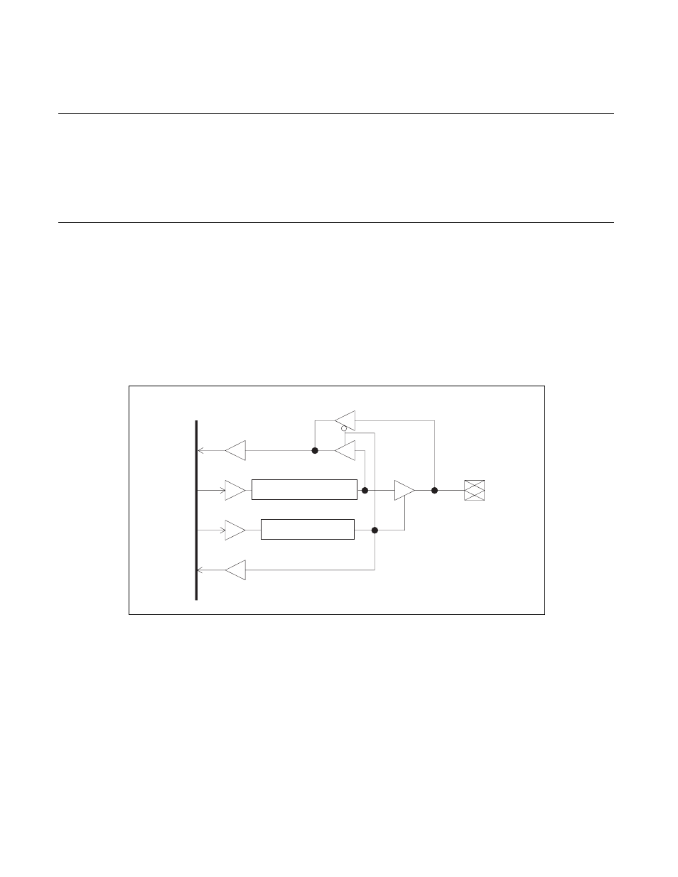
Figure 10.1-1 is a block diagram of the I/O ports.
Figure 10.1-1 I/O Port Block Diagram
Internal data bus
Port data register read
Port data register write
Port direction register write
Port direction register read
Port data register
Pin
Port direction register
