Reception and transmission data register (rdr/tdr) – FUJITSU F2MCTM-16LX User Manual
Page 415
399
CHAPTER 20 LIN-UART
20.4.4
Reception and Transmission Data Register (RDR/TDR)
Both RDR and TDR registers are located at the same address. At reading, it functions as
the reception data register. At writing, it functions as the transmission data register.
■
Reception Data Register (RDR)
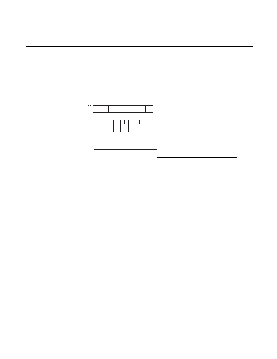
Figure 20.4-5 Transmission and Reception Data Registers (RDR/TDR)
RDR is the data buffer register for serial data reception. The serial data signal transmitted to the SINn pin is
converted in the shift register and stored in RDR register. When the data length is 7 bits, the uppermost bit
(RDR: D7) contains 0. When the data is stored in this register and the reception data full flag bit (SSR:
RDRF) is set to 1. If a reception interrupt request is enabled (SSR: RIE=1) at this point, a reception
interrupt occurs.
Read RDR when the RDRF bit of the serial status register (SSR) is 1. The RDRF bit is cleared
automatically to 0 when RDR is read. Also the reception interrupt is cleared if it is enabled and no error has
occurred.
Data in RDR is invalid when a reception error occurs (SSR: PE, ORE, or FRE = 1).
0 0 0 0 0 0 0 0
B
RDR0/TDR0: 000022
H
RDR1/TDR1: 00002A
H
bit
7
6
5
4
3
2
1
0
R/W R/W R/W R/W R/W R/W R/W R/W
D0
D1
D2
D3
D4
D5
D6
D7
Address
Initial value
bit7 to bit0
R/W
Data register
Read
Read from reception data register
Write
Write to transmission data register
R/W: Read/Write